 ALLPCB


Introduction to PCB Thickness
The thickness of a printed circuit board (PCB) is one of the most fundamental parameters in PCB design and manufacturing. It represents the distance from one surface of the board to the other, usually measured in millimeters. Despite appearing to be a simple specification, PCB thickness directly affects mechanical strength, electrical performance, heat dissipation, and manufacturing feasibility.
Standard PCB thicknesses typically range from 0.2mm to 3.2mm, with 0.6mm–1.6mm being the most commonly used in consumer electronics. This range provides a practical balance between cost, reliability, and functionality. However, as electronic devices become increasingly complex, niche applications now demand much thinner or thicker PCBs.
In this guide, we’ll dive into the characteristics of different PCB thicknesses, explore their impact on performance, and highlight how designers can make informed choices.
Characteristics and Applications of Different PCB Thicknesses
1. Below 0.6mm
Characteristics: Circuit board thickness below 0.6mm are extremely thin and flexible. They have relatively low mechanical strength on their own but are highly suitable for applications where flexibility is a key requirement. They also have good heat dissipation properties considering their small thermal mass.
Applications: Commonly used in flexible electronics such as wearable devices, flexible displays, and some medical implants where the PCB needs to conform to the shape of the body or other objects.
2. 0.6 - 1.6mm
Characteristics: This range offers a good balance of mechanical strength and flexibility. PCBs within this thickness range can support a moderate amount of component weight without significant warping. They also provide sufficient electrical isolation and are relatively easy to manufacture with standard processes.
Applications: Widely used in consumer electronics such as smartphones, tablets, laptops, and most general - purpose electronic devices. This thickness range is suitable for various circuit complexity levels, from simple single-layer boards to more complex multilayer boards.
3. Above 1.6mm
Characteristics: Thicker PCBs have excellent mechanical strength and can support heavy components. They have better heat-sinking capabilities due to their larger thermal mass. However, they are less flexible and may require more specialized manufacturing equipment for processing.
Applications: Found in power electronics, industrial control systems, and high-power applications where the PCB needs to handle large currents and dissipate significant amounts of heat. They are also used in applications where the PCB is subject to high mechanical stress, such as in automotive and aerospace electronics.
Suggested Reading: Is 1.6mm the Only Way? Exploring Standard PCB Thickness Options and Their Applications
Design and Manufacturing Factors Affecting PCB Thickness
1. Design Factors
Component Density and Weight: High-density designs with numerous and heavy components may require a thicker PCB to provide adequate support and prevent mechanical failures. For example, if a PCB has large power components or multiple heat sinks, a thicker substrate is often necessary.
Signal Integrity Requirements: In high-speed digital or RF circuits, the thickness affects impedance control. Thicker PCBs may have different impedance characteristics compared to thinner ones. Designers need to consider the impact on signal transmission and choose the thickness that ensures proper signal integrity.
Space Constraints: The available space within the final product enclosure limits the PCB thickness. In compact devices, a thinner PCB is preferred, while in larger systems with more room, a thicker PCB might be feasible.
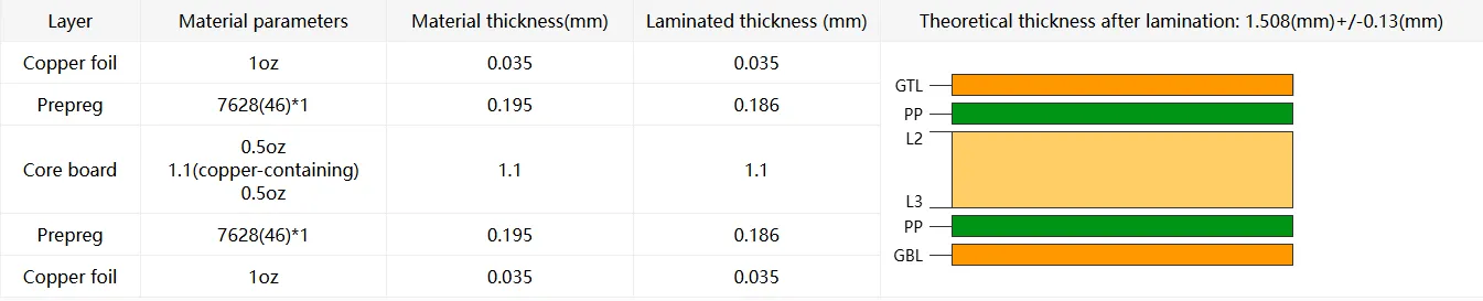
Multilayer Design: In multilayer PCBs, the thickness of each layer and the overall board thickness are determined by the number of layers required for routing signals, power distribution, and ground planes. The dielectric thickness between layers also affects electrical performance.
2. Manufacturing Factors
Etching and Plating Processes: Thicker PCBs may require longer etching times and more plating material to achieve the desired copper thickness and circuit patterns. The manufacturing process needs to be adjusted accordingly to ensure good quality.
Drilling and Routing: Thicker PCBs are more challenging to drill and route accurately. The equipment used may have limitations in handling thick boards, and the aspect ratio of drilled holes becomes more critical. Specialized drilling tools and techniques may be needed for thick PCBs.
Material Availability and Cost: Different thicknesses may have different availability and cost structures. Thicker PCBs may use more raw material, which can increase the custom PCB board cost. Manufacturers need to balance the desired thickness with the cost and availability of materials.
Suggested Reading: FR-4 vs. Alternatives: How Material Selection Impacts PCB Thickness Tolerance
Common Challenges in PCB Thickness
Warpage Issues
PCB warpage occurs due to uneven stress distribution, especially in multilayer or large-size boards. Excessive warpage can lead to assembly defects and reduced reliability.
Suggested Reading: Total PCB Thickness and Warpage Issue
Tolerance and Its Hidden Costs
Even small deviations in PCB thickness can cause manufacturing and assembly problems. Ignoring tolerance can result in misaligned components, failed impedance control, or even product recalls.
Suggested Reading: The Hidden Costs of Ignoring PCB Thickness Tolerance: A Manufacturer's Perspective
Special Considerations for Flex PCBs
Flexible PCBs require special attention to thickness selection because their applications often involve bending, folding, or twisting. Unlike rigid PCBs, thickness here dictates not only electrical performance but also mechanical durability. Getting this balance right ensures long-term reliability across diverse industries.
Performance vs. Bendability
Flex PCBs must balance bendability with consistent performance. Very thin circuits can bend tightly, making them ideal for wearables and compact electronics. However, they risk cracks, reduced insulation, or signal distortion after repeated flexing. Slightly thicker designs increase reliability but reduce flexibility, so the right trade-off depends on product requirements.
Suggested Reading: Beyond Bendability: How Flex PCB Thickness Impacts Performance and Reliability
Material Selection
The substrate and adhesive system largely define flex PCB thickness. Polyimide (PI) is the most common choice, offering stability under high temperatures and repeated bending. PET provides a cost-effective option but with limits in durability. Adhesive-less laminates can reduce thickness further, enhancing flexibility while still maintaining signal integrity.
Suggested Reading: Unlocking Flexibility: A Deep Dive into Flex PCB Thickness and Material Selection
Finding the Sweet Spot
Engineers often seek the “Goldilocks Zone” of flex PCB thickness—not too thin to risk damage, and not too thick to lose flexibility. This optimal range allows thousands of bending cycles while maintaining impedance stability. The best choice depends on whether the priority is space-saving design or long-term durability.
Suggested Reading: The Goldilocks Zone: Finding the Perfect PCB Thickness for Your Flex Circuit
How to Select the Appropriate PCB Thickness
1. Analyze the Application Requirements: Understand the end-use environment of the electronic product. For example, if it is a portable consumer device, a thinner PCB within the 0.6-1.6mm range might be suitable. For industrial applications with high-power components, a thicker PCB could be necessary.
2. Evaluate Component Characteristics: Consider the size, weight, and power dissipation of the components to be mounted on the PCB. Heavy or power-hungry components may demand a thicker substrate for mechanical support and heat dissipation.
3. Assess Signal Integrity Needs: In high-speed circuits, calculate the required impedance and analyze how different PCB thicknesses will affect signal transmission. Use simulation tools if possible to optimize the thickness for signal integrity.
4. Review Manufacturing Capabilities: Check the capabilities of the PCB manufacturing facility, including etching, plating, drilling, and routing equipment. Ensure that the chosen thickness can be manufactured with the available technology without sacrificing quality.
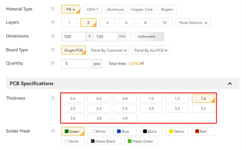
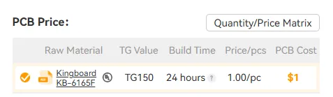
5. Consider Cost: Balance the performance requirements with the cost implications of different PCB thicknesses. Sometimes, a slightly thicker or thinner PCB may have a significant impact on the overall cost of the product. At ALLPCB, we offer 15 different thickness options from 0.4mm to 4.0mm, with prices starting from just $1 for 0.8-1.6mm thickness (for new users).
Suggested Reading: The Ultimate Guide to Standard PCB Thickness: Choosing the Right Fit for Your Project
Conclusion
PCB thickness is not just a physical dimension—it is a critical design parameter that influences signal performance, heat management, manufacturability, and product durability. From ultra-thin flex PCBs powering next-gen wearables to thick PCBs used in aerospace electronics, the right choice ensures long-term reliability.
By understanding application needs, material properties, and manufacturing limits, engineers can optimize PCB thickness for their projects. When in doubt, consult with PCB manufacturers like ALLPCB, who provide expert guidance and versatile options for every industry.


