ALLPCB


In the fast-evolving world of wearable technology, how do manufacturers pack powerful features into tiny, comfortable devices like smartwatches and fitness trackers? The answer lies in flexible PCB manufacturing. Flexible PCBs (Printed Circuit Boards) are the backbone of miniaturized, lightweight, and durable designs that power wearable tech. In this comprehensive guide, we’ll explore the role of flexible PCBs in wearable devices, focusing on their use in smartwatches and fitness trackers, the intricacies of miniaturized PCB design, the importance of high-density interconnects, and the unique challenges in flexible PCB assembly.
Whether you’re an engineer designing the next big wearable or a tech enthusiast curious about the technology behind your favorite gadget, this blog will provide actionable insights into how flexible PCBs enable cutting-edge innovation. Let’s dive into the details of this transformative technology.
What Are Flexible PCBs and Why Do They Matter for Wearable Tech?
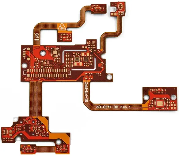
Flexible PCBs, often called flex circuits, are thin, lightweight circuit boards made from flexible materials like polyimide. Unlike traditional rigid PCBs, they can bend, fold, and twist without breaking, making them perfect for compact and dynamic applications like wearable technology. Their ability to conform to irregular shapes and fit into tight spaces is a game-changer for devices that need to be small, comfortable, and durable.
In wearable tech, such as smartwatches and fitness trackers, space is at a premium. These devices must house sensors, batteries, processors, and displays in a form factor that doesn’t feel bulky on the wrist. Flexible PCBs allow designers to maximize space efficiency while maintaining functionality. Their lightweight nature also reduces the overall weight of the device, enhancing user comfort.
The Role of Flexible PCBs in Smartwatches
When it comes to designing a smartwatch, every millimeter counts. Flexible PCBs for smartwatches are engineered to fit into the tiny, curved enclosures of these devices. They enable the integration of complex components like heart rate sensors, touchscreens, and wireless communication modules into a compact design.
One key advantage of using flexible PCBs in smartwatches is their ability to support dynamic movement. Smartwatches are often exposed to constant wrist motion, and a rigid board could crack under stress. Flexible PCBs, however, can withstand repeated bending without losing electrical connectivity. This durability ensures the device remains reliable even after months or years of use.
Additionally, flexible PCBs help reduce the thickness of the device. For instance, a typical smartwatch might use a multi-layer flexible PCB with a total thickness of just 0.2 mm, allowing manufacturers to create sleek, low-profile designs that appeal to consumers.
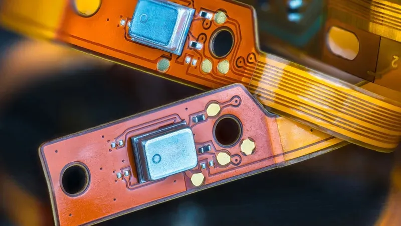
Flexible PCBs for Fitness Trackers: Powering Health Monitoring
Fitness trackers are another prime example of wearable tech that relies heavily on flexible PCBs. These devices often need to monitor vital signs like heart rate, steps, and sleep patterns while maintaining a slim, lightweight profile. Flexible PCBs for fitness trackers make this possible by providing a compact platform for sensors and microcontrollers.
A notable feature of flexible PCBs in fitness trackers is their ability to integrate high-density interconnects (HDI). HDI technology allows for tighter routing of electrical connections, meaning more components can fit into a smaller area. For example, a fitness tracker might use an HDI flexible PCB to pack a 32-bit processor, a 3-axis accelerometer, and an optical heart rate sensor into a board smaller than 20 mm x 10 mm.
Miniaturized PCB Design: The Heart of Wearable Innovation
Miniaturized PCB design is at the core of wearable technology. As devices get smaller, engineers face the challenge of maintaining performance while reducing size. Flexible PCBs are uniquely suited for this task because they can be folded or layered to fit into tight spaces without sacrificing functionality.
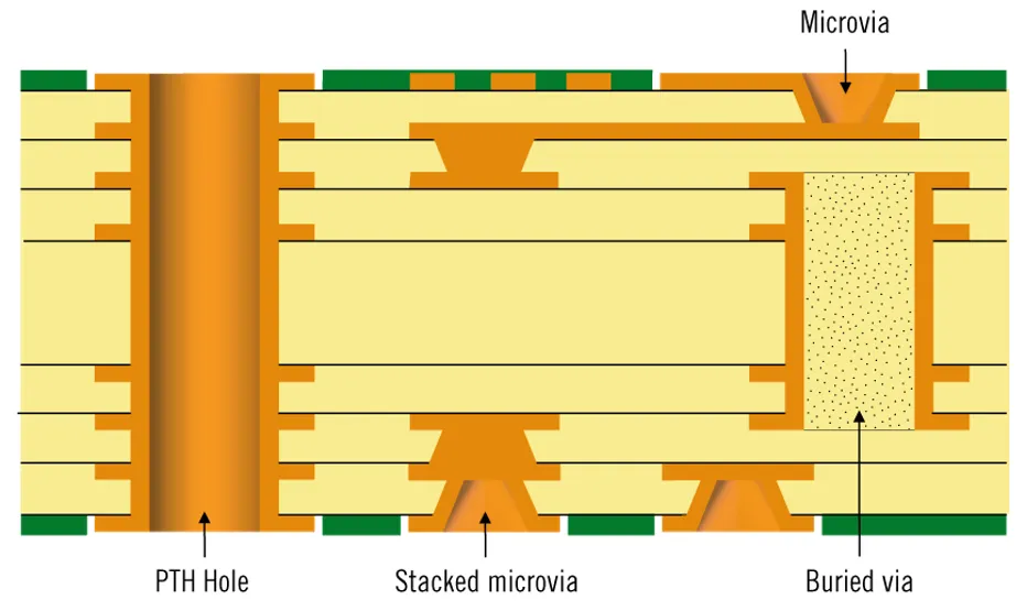
In miniaturized PCB design, every aspect must be optimized. Trace widths, for instance, are often reduced to as little as 0.05 mm to accommodate more connections in a smaller area. Similarly, via sizes (the tiny holes that connect different layers of the PCB) can be as small as 0.1 mm in diameter, enabling high-density layouts. These precise measurements ensure that even the smallest wearable device can handle complex tasks like real-time data processing and wireless communication.
However, miniaturization isn’t just about shrinking components. It’s also about managing heat and power efficiency. Wearable devices often operate on small batteries, so flexible PCBs must be designed to minimize power loss. For example, engineers might use low-resistance copper traces to reduce impedance, ensuring that signals travel efficiently with minimal energy waste.
High-Density Interconnects: Maximizing Performance in Tiny Spaces
High-density interconnects (HDI) are a critical feature of flexible PCBs used in wearable tech. HDI refers to a PCB design technique that increases the number of connections per unit area, allowing for more functionality in a smaller footprint. This is especially important for devices like smartwatches and fitness trackers, which need to support multiple features without increasing size.
In an HDI flexible PCB, layers are stacked with microvias (tiny connection holes) that enable precise routing between components. For instance, a smartwatch PCB might use a 6-layer HDI design to connect a processor, memory chip, and Bluetooth module, all within a board area of less than 15 mm x 15 mm. This high-density approach not only saves space but also improves signal integrity by shortening the distance signals need to travel, reducing latency and noise.
HDI technology also supports faster data transfer rates, which are essential for wearable devices that sync with smartphones or cloud services. By optimizing the PCB layout, engineers can achieve signal speeds of up to 5 Gbps in some wearable applications, ensuring seamless performance for users.
Flexible PCB Assembly Challenges: Overcoming Manufacturing Hurdles
While flexible PCBs offer incredible benefits for wearable tech, their assembly presents unique challenges. Unlike rigid PCBs, flexible boards are more delicate and require specialized handling during manufacturing to avoid damage. Let’s explore some of the key flexible PCB assembly challenges and how they are addressed.
1. Material Fragility: Flexible PCBs are made from thin, pliable materials that can tear or crease if mishandled. During assembly, manufacturers must use precise equipment to place components without stressing the board. For example, automated pick-and-place machines are often calibrated to apply minimal force when positioning tiny components like 0201 resistors (measuring just 0.6 mm x 0.3 mm).
2. Soldering Difficulties: Soldering components onto a flexible PCB is trickier than with rigid boards because the material can warp under heat. To prevent this, low-temperature soldering techniques or conductive adhesives are often used. Additionally, reflow ovens are set to specific profiles to ensure even heating, preventing thermal stress that could cause delamination.
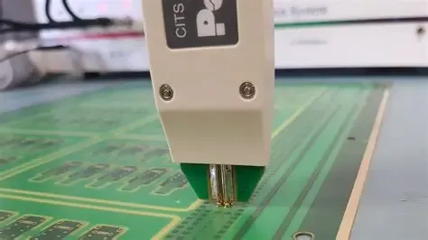
3. Component Density: The high component density in wearable tech PCBs means there’s little room for error during assembly. A slight misalignment can lead to short circuits or failed connections. Advanced vision systems and laser-guided placement tools are often employed to achieve accuracy down to 0.01 mm, ensuring reliable performance.
4. Testing and Inspection: After assembly, flexible PCBs must be thoroughly tested to ensure they function under bending and flexing conditions. Specialized test fixtures simulate real-world usage, such as repeated wrist movements for a smartwatch, to verify durability. For instance, a flexible PCB might undergo 10,000 flex cycles during testing to confirm it won’t fail prematurely.
Despite these challenges, advancements in manufacturing technology are making flexible PCB assembly more efficient. At ALLPCB, we leverage state-of-the-art equipment and rigorous quality control processes to deliver high-quality flexible PCBs tailored for wearable tech applications.
Benefits of Flexible PCBs Beyond Miniaturization
While miniaturization is a primary driver for using flexible PCBs in wearable tech, their benefits extend far beyond size reduction. Here are some additional advantages that make them indispensable:
- Durability: Flexible PCBs can endure vibrations and mechanical stress, making them ideal for active lifestyles. A fitness tracker, for example, might experience constant motion during a workout, and a flexible PCB ensures consistent performance.
- Weight Reduction: Wearable devices need to be lightweight for user comfort. Flexible PCBs, often weighing less than 1 gram even with multiple layers, help achieve this goal.
- Cost Efficiency: By reducing the need for connectors and cables (since the PCB can bend to connect components directly), flexible PCBs can lower overall production costs in high-volume manufacturing.
- Design Freedom: Engineers have more flexibility to create innovative shapes and layouts, leading to unique wearable designs that stand out in the market.
Future Trends in Flexible PCB Manufacturing for Wearable Tech
The future of flexible PCB manufacturing looks promising as wearable tech continues to grow. Emerging trends include the use of advanced materials like graphene for even thinner and more conductive flex circuits. Additionally, the integration of flexible PCBs with stretchable electronics is on the horizon, allowing devices to conform even more closely to the human body.
Another exciting development is the rise of 3D-printed flexible PCBs, which could enable rapid prototyping and customization for wearable devices. As these technologies mature, we can expect even smaller, more powerful smartwatches and fitness trackers with enhanced capabilities like real-time health monitoring and augmented reality features.

Conclusion: Why Flexible PCBs Are the Future of Wearable Tech
Flexible PCB manufacturing is unlocking new possibilities in wearable technology, enabling the creation of smaller, lighter, and more durable devices. From flexible PCBs for smartwatches to those powering fitness trackers, this technology is at the heart of modern miniaturization. By leveraging miniaturized PCB design and high-density interconnects, engineers can pack incredible functionality into tiny spaces, while overcoming flexible PCB assembly challenges ensures reliability and performance.
At ALLPCB, we’re committed to supporting the wearable tech industry with cutting-edge flexible PCB solutions. Whether you’re designing the next generation of smartwatches or pioneering health-focused fitness trackers, our expertise in flexible PCB manufacturing can help bring your vision to life. Embrace the power of miniaturization and let flexible PCBs shape the future of wearable innovation.