 ALLPCB


If you're looking for the ideal PCB gold finger thickness, the answer depends on your specific needs. For high insertion cycles, a thickness of 30-50 microinches (0.76-1.27 micrometers) of gold over a nickel underlayer is often recommended to ensure durability. For low contact resistance, a minimum of 10-20 microinches (0.25-0.51 micrometers) can suffice, though thicker plating enhances performance. Standards like IPC-6012 suggest a minimum of 30 microinches for Class 2 and 3 boards, but costs rise significantly with thicker gold layers—sometimes by 10-20% of the total PCB cost. Measurement techniques, such as X-ray fluorescence (XRF), ensure precision in verifying thickness. In this guide, we'll dive deep into balancing cost and performance, covering standards, applications, and practical tips for optimizing gold finger thickness.
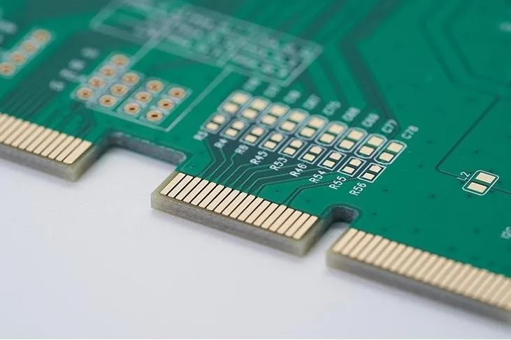
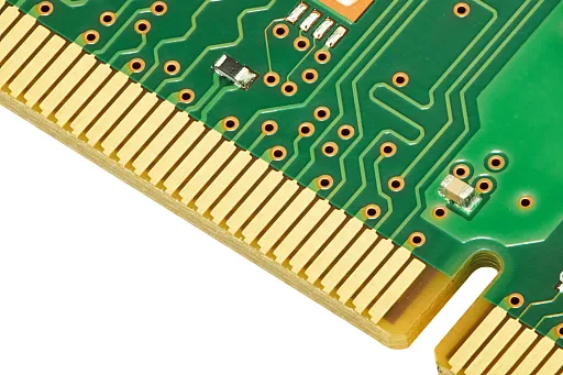
What Are PCB Gold Fingers and Why Do They Matter?
Gold fingers are the gold-plated connectors on the edges of a printed circuit board (PCB). They act as the interface between the PCB and other components, such as sockets or slots in devices like computers, graphics cards, or industrial equipment. Their primary role is to ensure reliable electrical connections, resist wear during repeated insertions, and prevent corrosion over time.
The thickness of the gold plating on these fingers is critical. Too thin, and the fingers may wear out quickly or fail to provide stable connections. Too thick, and the cost of production skyrockets without significant performance gains. Striking the right balance is essential for engineers and designers who want to optimize both functionality and budget.
Understanding PCB Gold Finger Plating Thickness Standards
When designing PCBs with gold fingers, adhering to industry standards ensures reliability and compatibility. The most widely recognized standard is set by the Institute of Printed Circuits (IPC), specifically in the IPC-6012 specification for rigid PCBs. According to this standard:
- Class 1 Boards (General Electronics): Minimum gold thickness of 5-10 microinches (0.13-0.25 micrometers) over a nickel underlayer of 50-150 microinches (1.27-3.81 micrometers).
- Class 2 Boards (Dedicated Service Electronics): Minimum gold thickness of 30 microinches (0.76 micrometers) over nickel.
- Class 3 Boards (High-Reliability Electronics): Minimum gold thickness of 30-50 microinches (0.76-1.27 micrometers) for critical applications like aerospace or medical devices.
These standards provide a baseline, but the exact thickness often depends on the application. For instance, a consumer-grade device with infrequent insertions may work fine with thinner plating, while industrial equipment requiring thousands of insertion cycles demands thicker gold for durability.
It's worth noting that gold is always applied over a nickel barrier layer. Nickel prevents diffusion between the base copper and gold, ensuring long-term stability. A typical nickel thickness ranges from 50 to 200 microinches (1.27-5.08 micrometers), depending on the gold layer and application.
Gold Finger Thickness for High Insertion Cycles
Insertion cycles refer to how many times a PCB can be plugged into and removed from a connector without degrading the gold fingers. High insertion cycles are common in applications like memory modules, graphics cards, and test equipment, where boards are frequently connected and disconnected.
For such scenarios, a gold thickness of 30-50 microinches (0.76-1.27 micrometers) is often ideal. This range provides enough material to withstand wear from repeated contact. Some studies suggest that a gold layer of at least 30 microinches can handle up to 1,000 insertion cycles without significant degradation, assuming proper nickel underplating and connector design.
However, thicker gold isn't always better. Beyond 50 microinches, the additional thickness offers diminishing returns in durability while significantly increasing costs. Engineers must also consider the connector's design and the force applied during insertion, as excessive pressure can accelerate wear regardless of thickness.
Gold Finger Thickness for Low Contact Resistance
Contact resistance is the electrical resistance at the point where the gold finger meets the connector. Low contact resistance is crucial for maintaining signal integrity, especially in high-speed or high-current applications like data transfer or power delivery systems.
A gold thickness of 10-20 microinches (0.25-0.51 micrometers) is often sufficient for achieving low contact resistance in less demanding applications. Gold's excellent conductivity—approximately 70% of copper's—ensures minimal resistance even at thinner layers. However, for high-performance boards, a thickness of 30 microinches or more can further reduce resistance and improve reliability, especially under varying environmental conditions like humidity or temperature fluctuations.
It's also important to maintain a smooth, uniform gold surface. Pinholes or uneven plating can increase contact resistance, regardless of thickness. Proper manufacturing processes, including thorough cleaning and precise electroplating, are just as critical as the thickness itself.
Gold Finger Thickness Measurement Techniques
Accurately measuring gold finger thickness is essential to ensure compliance with design specifications and industry standards. Several techniques are commonly used in the industry, each with its own advantages:
- X-Ray Fluorescence (XRF): This non-destructive method uses X-rays to measure the thickness of gold and nickel layers. It's highly accurate, with a precision of ±1 microinch (±0.025 micrometers), and is widely used for quality control in PCB manufacturing.
- Cross-Sectional Analysis: This destructive method involves cutting a sample of the PCB and examining the gold layer under a microscope. While precise, it's typically used for validation during development rather than routine testing due to its invasive nature.
- Beta Backscatter: Another non-destructive technique, beta backscatter measures thickness by analyzing the reflection of beta particles. It's less common than XRF but can be useful for specific applications.
Manufacturers often rely on XRF for its speed and accuracy, ensuring that every batch of PCBs meets the required gold thickness. Regular testing also helps identify inconsistencies in the plating process, preventing potential failures in the field.

Effect of Gold Thickness on PCB Cost
Gold is one of the most expensive materials used in PCB manufacturing, so the thickness of the gold layer directly impacts the overall cost. Here's how it breaks down:
- Thin Layers (5-10 microinches): These are the most cost-effective, often used in low-end consumer electronics. They can keep additional costs to under 5% of the total PCB price.
- Moderate Layers (20-30 microinches): Common for mid-range applications, these thicknesses increase costs by approximately 5-10%, depending on the board size and gold finger area.
- Thick Layers (40-50 microinches or more): Used in high-reliability applications, thicker gold can raise costs by 10-20% or more. The price jump is due to both the material cost and the longer electroplating time required.
Beyond material costs, thicker gold layers may require more complex manufacturing processes, such as additional quality checks or specialized equipment, further driving up expenses. Engineers must weigh these costs against the performance benefits. For example, if a board only requires 100 insertion cycles, opting for 50 microinches of gold instead of 30 could be an unnecessary expense.
One cost-saving strategy is selective plating, where gold is applied only to the finger areas rather than the entire board. This approach can reduce material usage by up to 50% in some designs, significantly lowering costs without compromising performance.
Factors to Consider When Choosing Gold Finger Thickness
Selecting the right gold finger thickness involves balancing several factors beyond just cost and performance. Here are some key considerations:
- Application Environment: Boards exposed to harsh conditions, such as high humidity or corrosive environments, benefit from thicker gold to prevent oxidation and ensure longevity.
- Signal Requirements: High-speed or high-frequency signals may require specific thicknesses to maintain signal integrity and minimize resistance.
- Insertion Frequency: As discussed earlier, frequent insertions demand thicker plating to resist wear.
- Budget Constraints: For cost-sensitive projects, thinner gold with a robust nickel underlayer can still provide adequate performance.
Collaboration with your PCB manufacturer early in the design phase can help identify the optimal thickness for your specific needs. Providing detailed specifications and discussing application requirements ensures that the final product meets both performance and cost goals.
Best Practices for Designing PCB Gold Fingers
To maximize the effectiveness of gold fingers, follow these design and manufacturing best practices:
- Bevel the Edges: A beveled edge on gold fingers reduces wear during insertion and improves alignment with connectors. A 30-45-degree bevel is standard for most applications.
- Ensure Uniform Plating: Work with manufacturers to achieve consistent gold thickness across all fingers, avoiding weak spots that could lead to failures.
- Specify Nickel Underlayer: A nickel layer of at least 50 microinches (1.27 micrometers) is essential to prevent copper diffusion and enhance durability.
- Avoid Over-Plating: Excessively thick gold can lead to issues like cracking or peeling, especially if the plating process isn't controlled tightly.
These practices not only improve the performance of gold fingers but also help control costs by preventing rework or failures during production.
Conclusion: Striking the Right Balance for Your PCB Design
Choosing the right PCB gold finger thickness is a delicate balance between cost, performance, and application requirements. Whether you prioritize durability for high insertion cycles, low contact resistance for signal integrity, or cost savings for budget-conscious projects, understanding the impact of gold thickness is key. Industry standards like IPC-6012 provide a starting point, but tailoring the thickness to your specific needs—whether it's 10 microinches for basic applications or 50 microinches for high-reliability systems—ensures optimal results.
By leveraging precise measurement techniques like XRF and following best practices in design and manufacturing, you can achieve reliable, cost-effective PCB gold fingers. Remember to collaborate closely with your manufacturing partner to align on specifications and processes, ensuring that your final product delivers the performance you need without breaking the bank.
With this guide, you now have the tools to make informed decisions about PCB gold finger thickness, balancing cost and performance for your next project.


