ALLPCB


If you're looking for a reliable way to clean vias and remove resin smear in multilayer and high-density interconnect (HDI) PCBs, plasma etching for desmear is the go-to solution. This process ensures clean via walls for better electrical conductivity and long-term reliability, especially in complex designs with blind and buried vias. In this comprehensive guide, we'll explore how PCB plasma etching desmear works, its benefits for via cleaning and resin removal, and why it's essential for modern multilayer and HDI PCB manufacturing.
What is PCB Desmear and Why Does It Matter?
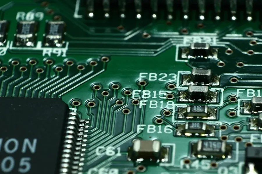
Desmearing is a critical step in PCB manufacturing that involves removing resin smear from the walls of drilled vias. During the drilling process in multilayer PCBs, heat and friction can cause resin from the substrate material to smear across the inner copper layers. This smear acts as an insulator, preventing proper electrical connections during plating. If left uncleaned, it can lead to poor conductivity, signal loss, or even complete circuit failure.
For HDI PCBs, which feature finer pitch vias and complex layer structures, desmearing is even more crucial. These boards often include blind vias (connecting an outer layer to an inner layer) and buried vias (connecting only internal layers), where resin smear can be harder to reach with traditional methods. Effective via cleaning ensures that electroless copper plating adheres properly, creating reliable connections across layers.
Traditional Desmear Methods vs. Plasma Etching
Historically, desmearing has been done using wet chemical processes, such as potassium permanganate solutions. While effective to some extent, these methods have drawbacks. They can be inconsistent, especially in microvias, and may damage or over-etch the copper layers. Additionally, wet chemistry involves hazardous materials, increasing waste disposal costs and safety risks in the workplace.
Plasma etching, on the other hand, uses ionized gas to remove resin smear without the risks associated with chemicals. This dry process offers precision and uniformity, making it ideal for complex multilayer PCBs and HDI designs. Unlike chemical methods, plasma etching does not weaken or etch the copper, ensuring the integrity of the inner layers remains intact.
How Does Plasma Etching Work for PCB Desmear?
Plasma etching involves placing the PCB in a vacuum chamber where a gas mixture, often containing oxygen or a combination of oxygen and other gases, is ionized to form plasma. This plasma reacts with the organic resin smear on the via walls, breaking it down into volatile compounds that are easily removed from the chamber. The result is a clean, smear-free surface ready for plating.
The process is highly controllable, allowing manufacturers to target specific areas without affecting the surrounding materials. For instance, in HDI PCBs with microvias as small as 0.1 mm in diameter, plasma etching can clean even the tiniest structures without over-etching. This precision is vital for maintaining signal integrity, especially in high-frequency applications where impedance mismatches can degrade performance. Typical impedance values in such designs are kept around 50 ohms to ensure signal speeds remain consistent, often exceeding 1 GHz in RF and microwave boards.
Another advantage is surface activation. Plasma treatment not only removes resin but also roughens the via walls slightly, improving adhesion for subsequent electroless copper plating. This enhances the reliability of connections, reducing the risk of delamination or failure over time.
Benefits of Plasma Etching for Via Cleaning in Multilayer and HDI PCBs
Plasma etching offers numerous advantages over traditional methods, making it a preferred choice for modern PCB fabrication. Let's break down the key benefits:
- Uniform Cleaning: Plasma etching provides consistent desmear across all vias, regardless of size or location on the board. This is especially important for HDI PCBs with dense via patterns.
- Access to Blind and Buried Vias: Unlike wet chemistry, which struggles to penetrate small or hidden vias, plasma can effectively clean microvias, blind vias, and buried vias.
- No Damage to Copper: The process is gentle on copper inner layers, preserving their thickness and conductivity. This is critical for maintaining signal integrity in high-speed designs.
- Environmentally Friendly: Plasma etching eliminates the need for harsh chemicals, reducing hazardous waste and improving workplace safety.
- Compatibility with Advanced Materials: It works well with a variety of substrates, including FR4, polyimide, and PTFE, which are common in high-frequency and RF applications.
Applications of Plasma Etching Desmear in PCB Manufacturing
Multilayer PCBs
Multilayer PCBs, which can have anywhere from 3 to 40 layers or more, rely on through-holes and vias to connect components across layers. Resin smear in these vias can disrupt connectivity, leading to failures. Plasma etching ensures clean via walls, enabling reliable interlayer connections even in boards with high layer counts.
HDI PCBs
High-density interconnect (HDI) PCBs are designed for compact, high-performance electronics, often found in smartphones, tablets, and medical devices. These boards feature fine-pitch vias, often with diameters below 0.15 mm, and complex structures like stacked microvias. Plasma etching is essential for desmearing these tiny vias, ensuring proper plating and signal transmission at speeds up to 10 Gbps or higher in advanced designs.
Blind and Buried Vias
Blind vias connect an outer layer to one or more inner layers, while buried vias link only internal layers without reaching the surface. Both types are common in HDI designs to save space and improve routing density. Plasma etching excels at cleaning these vias, where traditional methods often fail due to limited access.
Key Considerations for Effective PCB Plasma Etching Desmear
To achieve optimal results with plasma etching for via cleaning and resin removal, several factors must be considered during the process:
- Gas Mixture: The choice of gas, such as oxygen or a mix with nitrogen, affects the etching rate and uniformity. Manufacturers must select the right combination based on the resin type and substrate material.
- Process Time: Over-etching can damage the via walls or substrate, while under-etching may leave residual smear. Typical process times range from 5 to 15 minutes, depending on the board complexity.
- Power Settings: Plasma power, often between 100 and 500 watts, must be adjusted to balance etching efficiency with material safety. Higher power can speed up the process but risks overheating the board.
- Board Design: Complex designs with high via density or deep buried vias may require multiple etching cycles to ensure complete resin removal.
Challenges in Plasma Etching and How to Overcome Them
While plasma etching is highly effective, it’s not without challenges. One common issue is ensuring uniform etching across large boards. Variations in plasma distribution can lead to inconsistent cleaning, especially in densely packed areas. Using advanced equipment with uniform plasma distribution and rotating the board during etching can help address this.
Another challenge is handling advanced materials like PTFE, which may require specific gas mixtures or longer etching times due to their chemical stability. Testing different parameters during the setup phase can optimize the process for such materials.
Finally, plasma etching equipment requires a significant upfront investment and regular maintenance to ensure consistent performance. However, the long-term benefits of reduced waste, improved reliability, and compatibility with complex designs often outweigh the initial costs.
Why Choose Plasma Etching for Your PCB Projects?
For manufacturers and engineers working on multilayer or HDI PCBs, plasma etching for desmear offers unmatched precision and reliability. It ensures clean vias, even in the most intricate designs with blind and buried vias, leading to better electrical performance and durability. Whether you're designing boards for high-frequency applications with strict impedance control (e.g., 50 ohms for RF signals) or compact electronics requiring microvias, this technology delivers consistent results.
Moreover, plasma etching aligns with modern sustainability goals by minimizing the use of hazardous chemicals. This not only reduces environmental impact but also lowers operational costs related to waste management.
Conclusion: Elevating PCB Quality with Plasma Etching Desmear
Plasma etching has revolutionized PCB desmear and via cleaning, providing a precise, safe, and efficient solution for resin removal in multilayer and HDI PCBs. Its ability to clean even the smallest microvias, blind vias, and buried vias without damaging copper layers makes it indispensable for high-performance electronics. By adopting this technology, manufacturers can achieve cleaner connections, better plating adhesion, and enhanced signal integrity, all while supporting eco-friendly practices.
As PCB designs continue to push the boundaries of complexity and density, plasma etching will remain a cornerstone of reliable fabrication. Whether you're working on advanced RF boards or compact consumer electronics, understanding and leveraging this process can significantly elevate the quality of your products.