 ALLPCB


If you're dealing with unexpected PCB failures or performance issues, solder bridges might be the hidden culprit. These tiny, unintended connections between solder points can cause short circuits, leading to malfunctions or complete board failure. In this comprehensive guide, we'll explore PCB solder bridge defects, their causes, the consequences like electronic component short circuit, and how to diagnose and prevent them through PCB malfunction diagnosis and circuit board failure analysis. Let's dive into understanding this silent killer and how to protect your circuit boards from its devastating effects.
What Are Solder Bridges and Why Do They Matter?
Solder bridges are unintended connections formed by excess solder between two or more adjacent pads, pins, or traces on a printed circuit board (PCB). These bridges create electrical shorts, disrupting the intended flow of current and often leading to malfunction or failure. While they may seem like a small issue, their impact can be catastrophic, especially in high-stakes applications like medical devices or automotive electronics where reliability is critical.
The rise of miniaturization in electronics has made PCB solder bridge defects more common. As components get smaller and traces are placed closer together, even a tiny amount of excess solder—sometimes as little as 0.1mm thick—can bridge gaps and cause problems. Understanding and addressing solder bridges is essential for maintaining PCB performance and longevity.
Common Causes of Solder Bridge Defects
Solder bridges don't appear out of nowhere. Several factors during the design, manufacturing, and assembly processes can contribute to their formation. Identifying these causes is the first step in preventing them.
- Excess Solder Application: Applying too much solder during manual or automated soldering can create pools of molten solder that connect adjacent pads. This is especially common in hand-soldering where control over solder volume is less precise.
- Poor PCB Design: If pads or traces are placed too close together without adequate spacing, the risk of bridging increases. For instance, designs with pad spacing below 0.2mm are highly susceptible to solder bridges in surface-mount technology (SMT).
- Inadequate Solder Mask: A poorly applied or low-quality solder mask may fail to prevent solder from flowing onto unintended areas, leading to bridges between traces.
- Stencil Misalignment: During SMT assembly, if the stencil used for solder paste application is misaligned, paste can be deposited in the wrong areas, increasing the likelihood of bridges after reflow.
- Component Misplacement: Incorrectly placed components can force solder to spread unevenly during reflow, creating unintended connections.
- Thermal Issues: Uneven heating during the reflow process can cause solder to flow unpredictably, forming bridges between nearby points.
By addressing these root causes during the design and assembly stages, you can significantly reduce the risk of PCB solder bridge defects.
The Consequences of Solder Bridges on PCB Performance
The presence of a solder bridge can wreak havoc on a PCB, leading to a range of issues that impact performance and reliability. Understanding these solder bridge consequences highlights why they are often called the silent killer of PCB performance.
- Electronic Component Short Circuit: A solder bridge creates an unintended electrical connection, bypassing the intended circuit path. This can cause components to receive incorrect voltages or currents, leading to overheating or permanent damage. For example, a short circuit between power and ground pins can result in a current spike exceeding 5A in some cases, frying sensitive components.
- Signal Integrity Issues: In high-frequency circuits, a solder bridge can alter impedance and introduce noise, degrading signal quality. For instance, a bridge near a data line operating at 1GHz can cause signal crosstalk, leading to data errors.
- Complete Board Failure: If a solder bridge causes a critical short in a power supply line, the entire board may fail to operate. This is especially problematic in systems where redundancy isn't built in, resulting in costly downtime.
- Safety Hazards: In applications like automotive or medical electronics, a short circuit caused by a solder bridge can lead to dangerous outcomes, such as overheating or fires due to excessive current flow.
The financial impact of these issues can be significant. Reworking defective boards or replacing failed components often costs manufacturers thousands of dollars per batch, not to mention the loss of customer trust due to unreliable products.
How to Diagnose Solder Bridges in PCB Malfunction Analysis
Identifying solder bridges is a crucial part of PCB malfunction diagnosis and circuit board failure analysis. Since they are often microscopic, detecting them requires a combination of visual inspection and specialized testing methods.
Visual Inspection
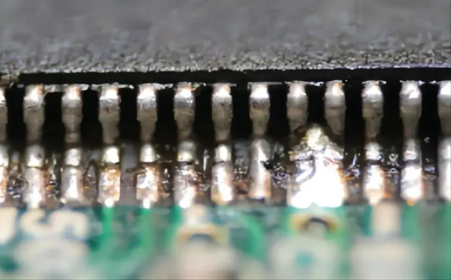
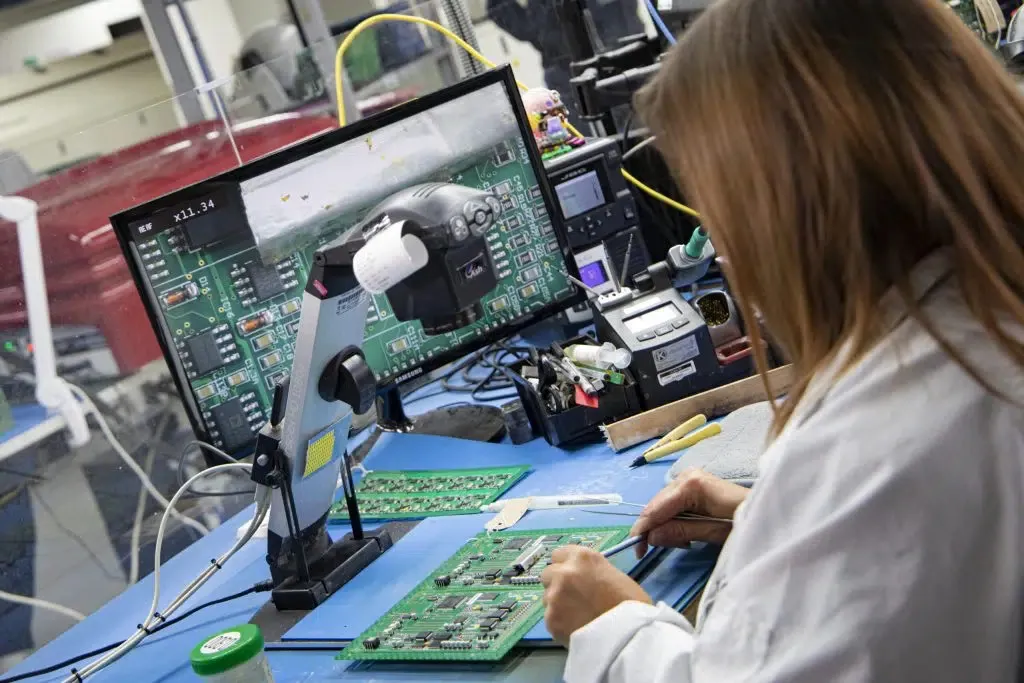
The simplest way to spot solder bridges is through careful visual inspection under magnification. Using a microscope with at least 10x magnification, look for shiny, continuous solder connections between adjacent pads or pins that shouldn't be connected. Pay close attention to densely populated areas of the board where components are packed tightly.
Automated Optical Inspection (AOI)
For larger-scale production, AOI systems use high-resolution cameras to scan PCBs for defects like solder bridges. These systems can detect anomalies in solder placement with an accuracy of up to 99.9%, making them invaluable for catching issues early in the manufacturing process.
X-Ray Inspection
In cases where solder bridges are hidden under components like ball grid arrays (BGAs), X-ray inspection is necessary. This method allows you to see through layers of the board and identify bridges that are not visible to the naked eye.
Electrical Testing
If visual methods don't reveal the issue, electrical testing can confirm the presence of a short circuit. Using a multimeter set to continuity mode, probe between adjacent pins or pads. A beep or low resistance reading (below 1 ohm) indicates a potential solder bridge. For more complex boards, in-circuit testing (ICT) can pinpoint shorts by comparing the board's electrical behavior to a known good reference.
Preventing Solder Bridges: Best Practices for PCB Design and Assembly
Prevention is always better than cure when it comes to solder bridges. By implementing best practices in design and manufacturing, you can minimize the risk of these defects and ensure reliable PCB performance.
Optimize PCB Design
Start with a design that reduces the likelihood of solder bridges. Ensure adequate spacing between pads and traces—aim for at least 0.25mm for SMT components. Use design rule checks (DRC) in your PCB layout software to flag potential issues before fabrication. Additionally, incorporate a high-quality solder mask to prevent solder from spreading to unintended areas.
Control Solder Paste Application
During assembly, use a well-designed stencil to apply solder paste precisely. Ensure the stencil apertures are appropriately sized—typically 80-90% of the pad area—to avoid excess paste. Regularly inspect and clean stencils to prevent misalignment or clogging.
Refine Soldering Techniques
For manual soldering, train technicians to use the correct amount of solder and to avoid overheating, which can cause solder to flow uncontrollably. In automated processes, optimize the reflow oven profile to ensure even heating, typically maintaining a peak temperature of 245°C for lead-free solder, with a time above liquidus of 60-90 seconds.
Implement Quality Control
Integrate AOI and X-ray inspection into your quality control process to catch solder bridges before boards leave the production line. Conduct random sampling and electrical testing on batches to ensure consistent quality.
Fixing Solder Bridges: Practical Solutions
If a solder bridge is detected, it’s often possible to fix it without scrapping the board. However, the repair process requires precision to avoid further damage.
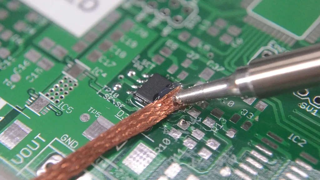
- Desoldering Braid: Use a desoldering braid (also called solder wick) to absorb excess solder. Place the braid over the bridge, apply a heated soldering iron (set to around 300°C), and let the braid soak up the solder until the connection is broken.
- Soldering Iron Tip: For small bridges, carefully use a fine-tip soldering iron to drag the excess solder away from the bridged area. Be cautious not to overheat components, as prolonged exposure to temperatures above 350°C can damage them.
- Hot Air Rework Station: For bridges under components, a hot air rework station can reflow the solder while you use tweezers to separate the connection. Maintain a temperature of 250-300°C and limit exposure time to under 30 seconds per area.
After repair, re-inspect the area visually and electrically to confirm the bridge is removed and no new issues have been introduced.
Conclusion: Protect Your PCBs from the Silent Killer
Solder bridges may be small, but their impact on PCB performance can be devastating. From causing electronic component short circuits to triggering complete board failures, the solder bridge consequences are too serious to ignore. By understanding their causes, using effective PCB malfunction diagnosis techniques, and implementing preventive measures, you can safeguard your circuit boards and ensure reliable operation.


