 ALLPCB


Are you looking to understand PCB edge plating and how it can benefit your projects? Whether you're a hobbyist or just starting out, PCB edge plating is a technique that can improve the performance of your printed circuit boards by enhancing electromagnetic shielding and creating reliable connections. In this comprehensive guide, we'll walk you through the basics of PCB edge plating, its benefits, and a step-by-step process to help you get started—even if you're working on projects at home. Let’s dive into this simple PCB edge plating tutorial designed for beginners and hobbyists.
What Is PCB Edge Plating?
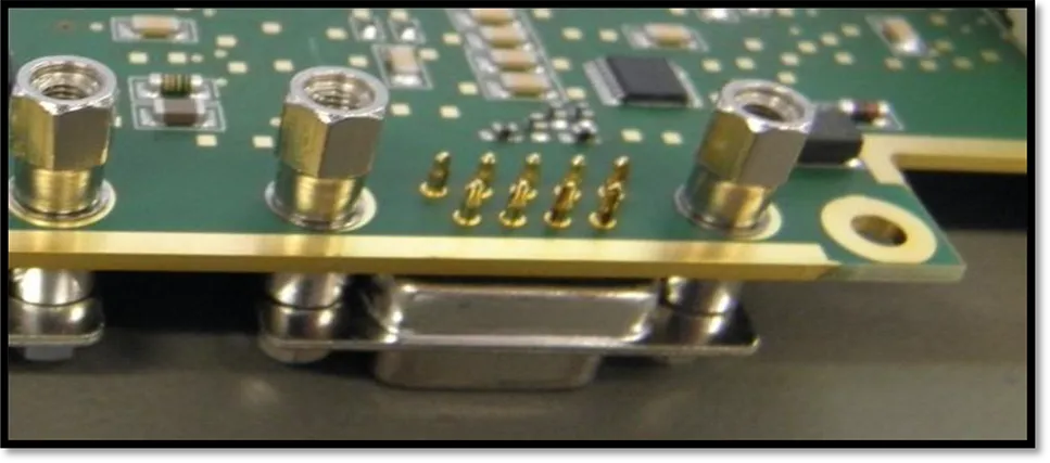
PCB edge plating, also known as side plating or castellation, is a process where a conductive metal layer, usually copper, is applied to the edges of a printed circuit board (PCB). This plating extends from the top to the bottom surface along one or more edges of the board, creating a continuous conductive path. This technique is often used to shield the board from electromagnetic interference (EMI), improve grounding, or create direct connections to enclosures or other components.
For beginners, think of edge plating as a protective and functional "wrap" around the sides of your PCB. It’s especially useful in high-frequency applications where signal integrity is critical, as it helps reduce noise and interference. If you're a hobbyist experimenting with RF (radio frequency) designs or multilayer boards at home, learning about PCB edge plating can take your projects to the next level.
Why Use PCB Edge Plating? Benefits for Beginners and Hobbyists
Before we get into the step-by-step guide, let’s explore why PCB edge plating is worth considering for your projects. Here are some key benefits that make it a valuable technique, even for simple PCB edge plating at home:
- EMI Shielding: Edge plating creates a conductive barrier around the PCB, reducing electromagnetic interference. This is crucial for high-frequency circuits where external signals can disrupt performance. For example, in RF designs, edge plating can help maintain signal integrity by blocking interference at frequencies up to 2.4 GHz, a common range for Wi-Fi applications.
- Improved Grounding: The plated edges provide a direct path to ground, ensuring better electrical stability. This can reduce noise in your circuit, which is especially helpful for sensitive analog designs.
- Connection to Enclosures: If your PCB is housed in a metal enclosure, edge plating allows for a seamless electrical connection between the board and the enclosure, enhancing overall shielding.
- Durability: Plating the edges protects the exposed copper from oxidation and physical damage during handling or transportation, which is a practical advantage for hobbyists working on multiple iterations of a design.
For hobbyists working at home, these benefits mean that even small-scale projects can achieve professional-grade performance with minimal additional effort. Now, let’s move on to how you can incorporate PCB edge plating into your designs.
Applications of PCB Edge Plating for Hobbyists
PCB edge plating isn’t just for industrial or complex designs—it has practical uses for hobbyists too. Here are a few scenarios where this technique can be applied in your home projects:
- RF and Wireless Projects: If you’re building a Wi-Fi module or a Bluetooth device, edge plating can help minimize interference and maintain signal quality.
- Multilayer Boards: For more advanced hobbyists creating multilayer PCBs, edge plating shields internal layers from external noise, ensuring cleaner operation.
- Custom Enclosures: If you’re designing a PCB to fit into a custom metal case (like for a portable gadget), edge plating ensures a solid connection between the board and the enclosure for grounding purposes.
Step-by-Step Guide to PCB Edge Plating for Beginners
Now that you understand the basics and benefits, let’s walk through a PCB edge plating tutorial tailored for beginners and hobbyists. While the actual plating process is typically done during manufacturing, as a designer, you need to prepare your PCB design files correctly to ensure the plating is applied as intended. Below are the steps to guide you through designing for edge plating and understanding the process. Note that for hobbyists working at home, you’ll likely need to collaborate with a PCB manufacturer for the actual plating, but we’ll also touch on DIY considerations.
Step 1: Plan Your Design with Edge Plating in Mind
Before you start designing your PCB, decide where edge plating is needed. Typically, it’s applied along one or more edges of the board, depending on your project’s requirements. For example, if you’re working on an RF project, you might want plating along all edges for maximum EMI shielding.
Keep these design tips in mind:
- Ensure that the edges to be plated are free of components or traces that could interfere with the plating process. Maintain a clearance of at least 0.8 mm between copper traces on non-connection layers and the board’s edge.
- Decide if you need single-axis (one edge) or multi-axis (multiple edges) plating based on your shielding or connection needs.
Step 2: Use PCB Design Software to Define Edge Plating Areas
Most PCB design software allows you to specify areas for edge plating. Here’s how to do it:
- Create a layer or outline in your design software to mark the edges where plating should be applied. This is often done in the board outline or a dedicated mechanical layer.
- Add annotations or notes in your design files to clearly indicate which edges require plating. This ensures the manufacturer understands your intent.
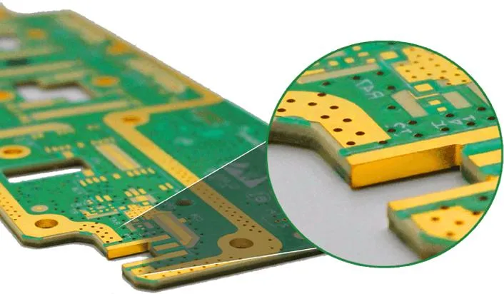
- If your design includes castellated holes (half-cut holes along the edge for mounting or connections), ensure they align with the plated edges for consistency.
Step 3: Choose the Right Material and Specifications
For beginners, understanding material choices is important. Edge plating is usually done with copper, followed by a surface finish like ENIG (Electroless Nickel Immersion Gold) to prevent oxidation. When working with a manufacturer, specify the following:
- Copper Thickness: Standard copper thickness for edge plating is around 1 oz (35 micrometers), but for high-current applications, you might opt for 2 oz (70 micrometers).
- Surface Finish: ENIG is a common choice for its durability and corrosion resistance, ensuring the plated edges last longer.
Step 4: Collaborate with a Manufacturer for Fabrication
For most hobbyists, PCB edge plating isn’t a process you can do at home due to the specialized equipment and chemicals required. Instead, you’ll need to work with a PCB fabrication service. Here’s how to ensure a smooth process:
- Export your design files (Gerber files) and include a detailed fabrication note specifying which edges need plating.
- Communicate with the manufacturer about any gaps or breaks in the plating. For instance, during production, manufacturers often leave small unplated sections (called “rout tabs”) where the board is held in a panel. These gaps are typically less than 1 mm wide and won’t affect performance in most cases.
- Review the manufacturer’s design guidelines for edge plating to avoid errors. Some may have specific requirements for clearance or edge preparation.
Step 5: DIY Edge Plating at Home (Optional, Experimental)
If you’re a hobbyist determined to try simple PCB edge plating at home, be aware that this is an experimental approach and not as reliable as professional manufacturing. Here’s a basic outline of how you might attempt it, though safety and precision are major concerns:
- Materials Needed: Copper sulfate solution, a power supply for electroplating, conductive paint, and protective gear (gloves, goggles).
- Process: Clean the PCB edges thoroughly, apply conductive paint to the areas you want to plate, and use an electroplating setup to deposit copper onto the edges. This process requires a controlled environment and precise voltage (typically 2-3 volts) to avoid damaging the board.
- Caution: Working with chemicals and electricity can be dangerous. This method is not recommended for beginners without proper training or equipment, as it can result in uneven plating or damage to your PCB.
For most hobbyists, it’s safer and more cost-effective to rely on professional services for edge plating rather than attempting it at home.
Step 6: Inspect the Finished PCB
Once you receive your PCB from the manufacturer (or complete your DIY attempt), inspect the edge plating for quality. Look for:
- Uniform copper coverage along the specified edges without gaps (except for rout tabs).
- No peeling or flaking of the plating, which could indicate poor adhesion.
- Proper alignment with any castellated holes or connection points.
If there are issues, contact the manufacturer to discuss corrections or adjustments for future orders.
Design Considerations for PCB Edge Plating
To ensure success with PCB edge plating, especially as a beginner or hobbyist, keep these design considerations in mind:
- Board Thickness: Edge plating works best on boards with a thickness of 1.6 mm or more, as thinner boards may not support uniform plating.
- Edge Clearance: Maintain a clearance of at least 0.5-0.8 mm between internal traces and the board edge to prevent accidental shorting during plating.
- Cost Impact: Edge plating adds to the manufacturing cost, typically increasing the price by 10-20% depending on the complexity and number of edges. Plan your budget accordingly.
Common Challenges and How to Avoid Them
As a beginner, you might face a few challenges with PCB edge plating. Here’s how to handle them:
- Design File Errors: Double-check your Gerber files and fabrication notes to ensure the manufacturer knows exactly where to apply plating. Use a design review tool if available in your software.
- Uneven Plating: This can happen if the board edge isn’t properly prepared. Ensure your design adheres to manufacturer guidelines for edge clearance and surface finish.
- Signal Interference: If edge plating is too close to high-speed signal traces, it might cause unintended capacitance. Keep sensitive traces away from plated edges or consult with an experienced designer for advice.
Tips for Hobbyists Working on PCB Edge Plating at Home
If you’re a hobbyist looking to integrate edge plating into your projects, here are some practical tips to make the process smoother:
- Start with small, simple projects to test edge plating before moving to complex designs.
- Use online forums and communities to learn from other hobbyists who have successfully implemented edge plating in their designs.
- Choose a reliable fabrication service with clear guidelines for edge plating to avoid miscommunication or errors in production.
Conclusion: Elevate Your PCB Designs with Edge Plating
PCB edge plating is a powerful technique that can significantly enhance the performance of your circuit boards, even for beginners and hobbyists working at home. By providing EMI shielding, improving grounding, and ensuring durable connections, edge plating is a valuable addition to projects like RF modules, multilayer boards, and custom enclosures. With this step-by-step PCB edge plating tutorial, you now have the knowledge to design for edge plating and collaborate with manufacturers to achieve professional results—or experiment cautiously with DIY methods if you’re feeling adventurous.
Remember to plan your design carefully, communicate clearly with your fabrication partner, and inspect the final product for quality. Whether you’re just starting out or looking to refine your skills, mastering simple PCB edge plating can open up new possibilities for your electronic projects. Take the first step today and see how this technique can improve your designs!


