 ALLPCB


In the fast-paced world of electronics manufacturing, precision is everything. High-precision PCB drilling, especially through laser technology, is transforming how printed circuit boards (PCBs) are made. This blog dives deep into how laser drilling enhances accuracy, supports high-density interconnect (HDI) designs, and outperforms traditional mechanical drilling. If you're searching for insights on high precision laser drilling PCB manufacturing, laser drilling accuracy PCB, laser drilling HDI PCB, laser drilling vs mechanical drilling precision, or laser drilling process control, you're in the right place. Let’s explore how this cutting-edge technology is shaping the future of electronics.
What is High-Precision PCB Drilling and Why Does It Matter?
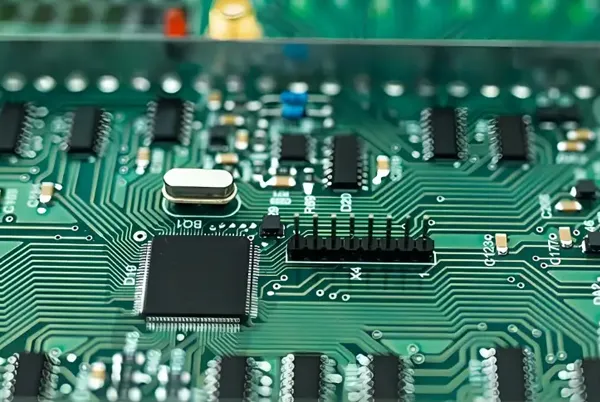
PCB drilling is the process of creating holes, or vias, in a printed circuit board to connect different layers or mount components. These holes must be incredibly precise to ensure the board functions correctly. High-precision drilling is critical as electronics become smaller and more complex. A single misplaced or oversized hole can disrupt signal integrity, leading to failures in devices like smartphones, medical equipment, or automotive systems.
Laser technology has emerged as a game-changer in this field. Unlike traditional methods, laser drilling offers unmatched accuracy and control, making it ideal for modern PCB designs. This is especially true for HDI PCBs, where space is limited, and vias need to be as small as 0.1 mm or less in diameter.
The Basics of Laser Drilling in PCB Manufacturing
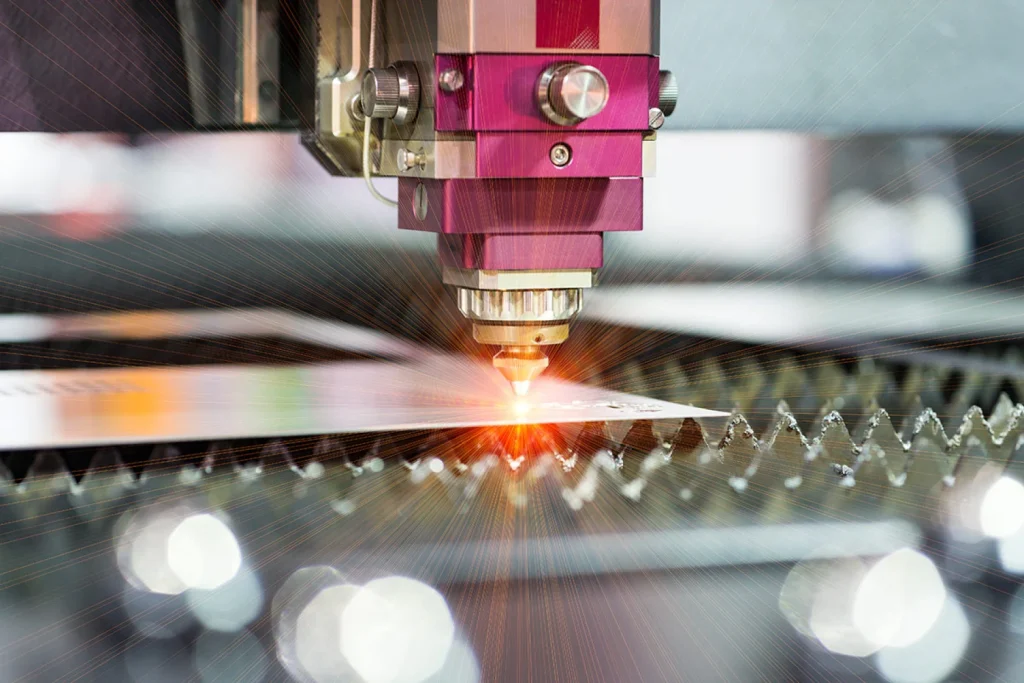
Laser drilling uses focused beams of light to remove material from a PCB with extreme precision. The process involves directing a laser, often a CO2 or UV type, onto the board to vaporize or ablate tiny areas of material. This creates clean, accurate holes without the physical contact required by mechanical drills.
One key advantage of high precision laser drilling PCB manufacturing is its ability to create microvias—tiny holes often less than 0.15 mm in diameter. These are essential for HDI PCBs, which pack more components into smaller spaces. Laser drilling can achieve tolerances as tight as ±0.01 mm, ensuring that even the smallest vias align perfectly with design specifications.
Key Benefits of Laser Drilling Accuracy in PCBs
The accuracy of laser drilling is a standout feature that sets it apart from other methods. Here’s why laser drilling accuracy PCB manufacturing is so impactful:
- Pinpoint Precision: Laser beams can be focused to a spot size as small as 0.02 mm, allowing for exact hole placement and size. This is crucial for maintaining signal integrity at high frequencies, where even a 0.05 mm deviation can cause impedance mismatches.
- Consistency: Lasers deliver uniform results across thousands of holes, reducing the risk of defects. For example, in a board with 10,000 vias, laser drilling maintains consistent quality, unlike mechanical methods that may wear down over time.
- Non-Contact Process: Since there’s no physical tool touching the board, there’s less risk of damage or misalignment, preserving the delicate layers of the PCB.
These benefits translate to higher reliability in end products, whether it’s a wearable device or an aerospace system. Precision ensures that signals travel at optimal speeds—often exceeding 10 Gbps in modern designs—without interference.
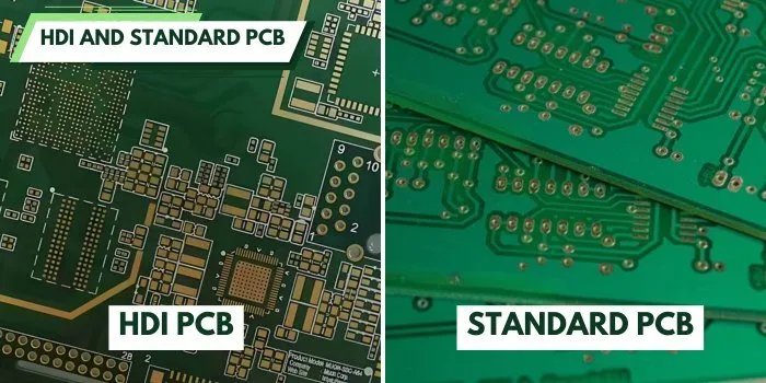
Laser Drilling and HDI PCBs: A Perfect Match
High-density interconnect (HDI) PCBs are the backbone of compact, high-performance electronics. They require smaller vias and finer traces to fit more functionality into limited space. Laser drilling HDI PCB technology is uniquely suited for this task.
Traditional drilling struggles with the microvias needed for HDI designs, often limited to holes larger than 0.3 mm. Laser drilling, on the other hand, can create vias as small as 0.05 mm, allowing for denser layouts. This capability supports advanced stacking techniques, where multiple layers are connected through blind or buried vias, reducing board size by up to 30% compared to standard designs.
In practical terms, this means a smartphone PCB can house more components without increasing its footprint. It also improves signal integrity by shortening connection paths, which is vital for high-speed applications operating at frequencies above 5 GHz.
Laser Drilling vs Mechanical Drilling: Precision Comparison
When it comes to laser drilling vs mechanical drilling precision, the differences are stark. Mechanical drilling uses rotating bits to physically cut through the PCB material. While effective for larger holes, it falls short in modern applications. Let’s break down the comparison:
- Hole Size: Mechanical drills are limited to holes around 0.2-0.3 mm in diameter at best. Laser drilling can achieve holes as small as 0.05 mm, making it ideal for HDI and microvia applications.
- Accuracy: Mechanical drills can deviate by ±0.05 mm or more due to tool wear or vibration. Laser systems maintain tolerances within ±0.01 mm, ensuring precise alignment across layers.
- Material Impact: Mechanical drilling can cause burrs or delamination, especially in fragile materials like thin laminates. Laser drilling produces clean edges with minimal thermal damage when properly controlled.
- Speed: For high-volume production, lasers can drill thousands of vias per second—some systems reach speeds of 9,000 vias per second—while mechanical drills are slower and require tool changes.
While mechanical drilling may still be suitable for simpler, larger-scale boards, laser technology is the clear choice for precision-driven projects. It reduces error rates by up to 40% in complex designs, directly impacting manufacturing yield and cost efficiency.
Laser Drilling Process Control: Ensuring Quality and Reliability
Laser drilling process control is critical to achieving consistent results. Advanced systems use real-time monitoring and feedback to adjust parameters like beam intensity, pulse duration, and focus. Here’s how control mechanisms elevate the process:
- Beam Focus and Power: Systems automatically adjust the laser’s focus to maintain a spot size of 0.02-0.05 mm, ensuring uniform hole depth and diameter. Power levels are fine-tuned to avoid overheating, which could damage dielectric layers.
- Material Sensing: Modern laser equipment detects material thickness and composition, adapting settings to prevent over-drilling. For instance, drilling through a 0.1 mm copper layer requires different parameters than a 0.5 mm substrate.
- Positioning Accuracy: High-end machines use vision systems to align the laser with design coordinates, achieving placement accuracy within 0.005 mm. This is essential for multi-layer boards where vias must align across 8 or more layers.
Effective process control minimizes defects like incomplete vias or charring, which can compromise a board’s performance. It also boosts throughput, allowing manufacturers to produce complex boards at scale without sacrificing quality.
Applications of Laser Drilling in Electronics Manufacturing
Laser drilling is unlocking new possibilities across various industries. Its ability to create tiny, precise holes supports innovation in:
- Consumer Electronics: Smartphones, tablets, and wearables rely on HDI PCBs with microvias for compact, high-speed designs. Laser drilling enables boards with trace widths below 0.1 mm, supporting data rates up to 25 Gbps.
- Automotive Systems: Advanced driver-assistance systems (ADAS) and electric vehicle controls use multi-layer PCBs. Laser-drilled vias ensure reliable connections in harsh environments, withstanding vibrations and temperature swings from -40°C to 85°C.
- Medical Devices: Implantable devices and diagnostic tools need miniature PCBs. Laser drilling creates vias small enough to fit within a 5 mm x 5 mm board, maintaining functionality without bulk.
- Aerospace and Defense: High-reliability applications demand flawless signal transmission. Laser drilling supports boards with up to 20 layers, ensuring zero defects in critical systems.
These applications highlight why laser technology is becoming the standard for high-precision PCB manufacturing. It meets the demands of modern electronics, where size, speed, and reliability are non-negotiable.
Challenges and Considerations in Laser Drilling
While laser drilling offers incredible benefits, it’s not without challenges. Understanding these can help manufacturers optimize their processes:
- Cost: Laser drilling equipment is more expensive than mechanical systems, with initial investments often exceeding $500,000 for high-end models. However, the long-term savings from reduced defects and higher yields often justify the cost.
- Thermal Effects: If not controlled, laser heat can cause charring or damage to nearby materials. Advanced cooling and pulse control mitigate this, limiting heat-affected zones to under 0.02 mm.
- Material Limitations: Some thick or highly reflective materials may resist laser drilling, requiring hybrid approaches with mechanical methods for certain boards.
Despite these hurdles, ongoing advancements in laser technology are addressing these issues, making it more accessible and versatile for PCB production.
The Future of Laser Drilling in PCB Manufacturing
The future of high precision laser drilling PCB manufacturing looks promising. As electronics continue to shrink and performance demands grow, laser technology will play an even bigger role. Emerging trends include:
- Ultra-Fast Lasers: New femtosecond lasers reduce thermal impact, drilling holes with near-zero heat-affected zones, ideal for ultra-thin substrates under 0.05 mm thick.
- Automation: Integration with AI and machine learning enhances process control, predicting and adjusting for variables in real-time to maintain 100% accuracy.
- 5G and Beyond: With 5G and future 6G networks requiring PCBs to handle frequencies above 30 GHz, laser drilling will be essential for creating vias that minimize signal loss.
These innovations signal that laser drilling will remain at the forefront of electronics manufacturing, driving efficiency and enabling next-generation devices.
Conclusion: Embracing Laser Technology for Superior PCB Performance
Laser drilling is revolutionizing electronics manufacturing by delivering unmatched precision, supporting HDI designs, and outperforming mechanical methods. Whether it’s the pinpoint accuracy of laser drilling for PCB vias, the ability to handle complex HDI layouts, or the superior control over the drilling process, this technology is setting new standards. For industries where reliability and performance are critical, adopting high precision laser drilling PCB manufacturing is not just an option—it’s a necessity.
By leveraging laser technology, manufacturers can meet the challenges of modern electronics, from shrinking device sizes to increasing data speeds. As advancements continue, laser drilling will only become more integral to creating the cutting-edge devices that power our world.


