 ALLPCB


In the world of electronics design, engineers are increasingly turning to halogen-free PCBs to meet environmental standards and ensure safer, more sustainable products. But what exactly are halogen-free PCBs, and why should you consider them for your next project? In this comprehensive guide, we’ll explore everything you need to know about halogen-free PCB design, including the materials used, their benefits, the environmental impact of halogenated PCBs, and tips for choosing the right halogen-free laminates. Whether you’re designing for consumer electronics or industrial applications, this blog will provide actionable insights to help you make informed decisions.
What Are Halogen-Free PCBs?
Halogen-free PCBs are printed circuit boards made without materials containing halogens like chlorine, bromine, fluorine, iodine, or astatine. These elements are often found in traditional PCB laminates and flame retardants, but they can pose health and environmental risks when exposed to heat or fire. Halogen-free alternatives replace these substances with safer compounds, maintaining performance while reducing potential hazards.
For engineers, switching to halogen-free PCB design means aligning with global regulations like the Restriction of Hazardous Substances (RoHS) directive and addressing growing demands for eco-friendly electronics. Let’s dive deeper into why this shift matters and how it impacts your design process.
Why Choose Halogen-Free PCB Materials?
Halogen-free PCB materials are gaining traction for several reasons. They not only address environmental and safety concerns but also offer performance benefits that make them suitable for a wide range of applications. Here are the key reasons engineers are making the switch:
1. Environmental Safety
Traditional PCBs often contain halogenated flame retardants that release toxic fumes, such as dioxins, when burned or exposed to high temperatures. These fumes can harm both the environment and human health. Halogen-free materials significantly reduce this risk, making them a preferred choice for sustainable design. According to studies, manufacturing processes using halogen-free laminates can lower the global warming potential (GWP) of PCB production by up to 86% when combined with additive manufacturing techniques.
2. Compliance with Regulations
Global standards like RoHS and the International Electrotechnical Commission (IEC) guidelines (specifically IEC 61249-2-21) define limits for halogen content in electronics. For a PCB to be considered halogen-free, it must contain less than 900 ppm of chlorine or bromine and less than 1500 ppm of total halogens. Using halogen-free materials ensures compliance with these strict regulations, avoiding potential legal or market access issues.
3. Enhanced Thermal Stability
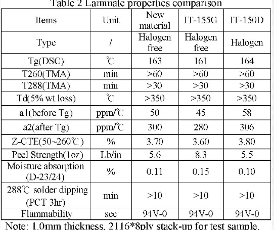
Halogen-free laminates are designed to withstand high temperatures, making them ideal for applications requiring robust thermal performance. Many halogen-free materials offer a glass transition temperature (Tg) ranging from 150°C to 170°C, compared to 130°C to 150°C for some traditional FR-4 laminates. This higher Tg ensures better reliability in high-heat environments like automotive or industrial electronics.
4. Improved Insulation Properties
Halogen-free materials often provide superior dielectric properties, which can enhance signal integrity in high-frequency applications. For instance, some halogen-free laminates have a dielectric constant (Dk) as low as 3.5 at 1 GHz, reducing signal loss compared to standard materials with a Dk of 4.0 or higher. This makes them a smart choice for RF and microwave designs.
Benefits of Halogen-Free PCBs for Engineers
The benefits of halogen-free PCBs extend beyond environmental compliance. They offer practical advantages that directly impact design, manufacturing, and end-product performance. Here’s a closer look at how these benefits can enhance your projects:
1. Safer Working Conditions
During manufacturing or in the event of a fire, halogen-free PCBs minimize the release of harmful gases. This creates safer conditions for workers in assembly lines and repair shops, as well as for end-users in case of product failure.
2. Market Competitiveness
With increasing consumer awareness about sustainability, products made with halogen-free materials can give your company a competitive edge. Many industries, including medical and consumer electronics, now prioritize eco-friendly components, making halogen-free PCBs a selling point.
3. Long-Term Reliability
Halogen-free laminates often exhibit better resistance to moisture and chemical degradation, extending the lifespan of the PCB. For example, some materials show a moisture absorption rate of less than 0.1%, compared to 0.2% for traditional options, reducing the risk of delamination in humid environments.
4. Versatility Across Applications
From smartphones to automotive control units, halogen-free PCBs are suitable for a wide range of uses. Their ability to meet high thermal and electrical demands ensures they can handle the rigors of modern electronics, whether operating at 5V for consumer devices or higher voltages in industrial systems.
Environmental Impact of Halogenated PCBs
Understanding the environmental impact of halogenated PCBs is crucial for engineers looking to adopt greener practices. Halogens, particularly bromine and chlorine, have been used in flame retardants for decades due to their effectiveness in preventing fires. However, their downsides are significant:
1. Toxic Emissions
When halogenated materials are exposed to heat or incinerated, they can release hazardous substances like hydrogen halides and dioxins. These pollutants contribute to air and soil contamination, posing risks to ecosystems and human health. For instance, dioxins are known to be carcinogenic and can persist in the environment for years.
2. Challenges in Recycling
Halogenated PCBs are harder to recycle due to the need for specialized processes to handle toxic byproducts. This often leads to improper disposal, further exacerbating environmental damage. In contrast, halogen-free materials are more compatible with standard recycling methods, supporting a circular economy.
3. Resource Depletion
The production of halogenated materials often relies on non-renewable resources and energy-intensive processes. Research indicates that electricity generation alone accounts for about 41% of the global warming potential in conventional PCB manufacturing. Switching to halogen-free alternatives can significantly cut down on resource use and carbon footprint.
Choosing Halogen-Free Laminates: Key Factors to Consider
Selecting the right halogen-free laminates for your PCB design requires careful evaluation of material properties, application needs, and cost considerations. Here are the main factors to keep in mind when choosing halogen-free laminates:
1. Material Composition
Halogen-free laminates typically use phosphorus-based or nitrogen-based flame retardants instead of halogenated compounds. Common base materials include modified epoxy resins or polyimide, often reinforced with glass fiber for strength. Ensure the material meets the halogen content thresholds defined by IEC standards (less than 900 ppm for individual halogens).
2. Thermal Performance
Check the glass transition temperature (Tg) and thermal decomposition temperature (Td) of the laminate. For high-reliability applications, opt for materials with a Tg above 150°C and a Td above 340°C to withstand soldering and operational heat. These values ensure the PCB remains stable under stress.
3. Electrical Properties
For high-frequency designs, prioritize laminates with a low dielectric constant (Dk) and low dissipation factor (Df). A Dk of 3.5 or lower and a Df of 0.005 or less at 1 GHz can minimize signal loss, which is critical for applications like 5G or IoT devices.
4. Mechanical Strength
Evaluate the tensile strength and flexibility of the laminate to ensure it can handle the mechanical stresses of assembly and use. Some halogen-free materials offer a tensile strength of up to 300 MPa, comparable to traditional FR-4, making them suitable for multilayer boards.
5. Cost vs. Performance
While halogen-free laminates can be more expensive—sometimes 10-20% higher than standard materials—their benefits in terms of compliance, safety, and reliability often justify the cost. Balance your budget with the specific requirements of your project to find the best fit.
Challenges in Halogen-Free PCB Design
While halogen-free PCBs offer numerous advantages, they come with certain challenges that engineers must address during design and manufacturing:
1. Higher Material Costs
As mentioned earlier, halogen-free materials can cost more due to the specialized compounds used as flame retardants. This may impact small-scale projects or budgets with tight constraints.
2. Processing Differences
Some halogen-free laminates require adjustments in fabrication processes, such as higher curing temperatures or longer processing times. For instance, certain materials need curing at 200°C for 90 minutes, compared to 180°C for 60 minutes for standard laminates. Ensure your manufacturing setup can accommodate these differences.
3. Limited Availability
Although the availability of halogen-free materials is increasing, not all suppliers stock a wide range of options. This can limit your choices for specific applications or lead to longer lead times.
How to Transition to Halogen-Free PCB Design
Moving to halogen-free PCB design doesn’t have to be overwhelming. Follow these steps to ensure a smooth transition:
- Assess Your Needs: Determine if halogen-free materials are necessary for your application based on regulatory requirements, environmental goals, or customer demands.
- Research Materials: Work with your supplier to identify halogen-free laminates that match your thermal, electrical, and mechanical specifications.
- Test Prototypes: Before full-scale production, build and test prototypes to evaluate performance under real-world conditions. Check for issues like delamination or signal integrity.
- Update Processes: Adjust your manufacturing parameters, such as soldering temperatures or drilling speeds, to suit the properties of halogen-free materials.
- Educate Your Team: Ensure your design and production teams understand the benefits and handling requirements of halogen-free PCBs to avoid errors.
Conclusion: The Future of Halogen-Free PCBs
As the electronics industry continues to prioritize sustainability and safety, halogen-free PCBs are becoming a standard choice for forward-thinking engineers. By understanding the benefits of halogen-free PCB materials, the environmental impact of halogenated alternatives, and the factors involved in choosing halogen-free laminates, you can design products that meet modern demands without compromising performance. While challenges like cost and processing differences exist, the long-term advantages of safer, eco-friendly designs make the transition worthwhile.
At ALLPCB, we’re committed to supporting engineers with high-quality, environmentally conscious solutions for every project. Whether you’re exploring halogen-free PCB design for the first time or looking to optimize an existing product, our expertise and resources are here to help you succeed. Embrace the future of electronics with confidence and make halogen-free PCBs a cornerstone of your next innovation.


