 ALLPCB


In a world increasingly reliant on electronics, the challenge of managing electronic waste, especially printed circuit boards (PCBs), has never been more critical. Traditional methods like incineration harm the environment by releasing toxic fumes and wasting valuable materials. So, how can we recycle PCBs sustainably? Advanced PCB recycling technologies, including pyrometallurgy, hydrometallurgy, and electrochemical processes, offer eco-friendly and efficient solutions for PCB material separation. In this blog, we’ll explore these cutting-edge methods, diving deep into how they work and why they’re essential for a greener future.
Why PCB Recycling Matters in Today’s World
PCBs are the backbone of nearly every electronic device, from smartphones to industrial machinery. However, when these devices reach the end of their life cycle, they often end up in landfills, posing serious environmental risks. PCBs contain hazardous substances like lead, mercury, and brominated flame retardants, which can leach into soil and water if not handled properly. At the same time, they’re packed with valuable metals like gold, silver, copper, and palladium—materials too precious to waste.
Advanced PCB recycling not only prevents pollution but also recovers these materials for reuse, reducing the need for mining and conserving natural resources. With global e-waste generation reaching over 50 million tons annually, adopting sustainable recycling methods is no longer optional; it’s a necessity. Let’s dive into the innovative technologies transforming PCB material separation.
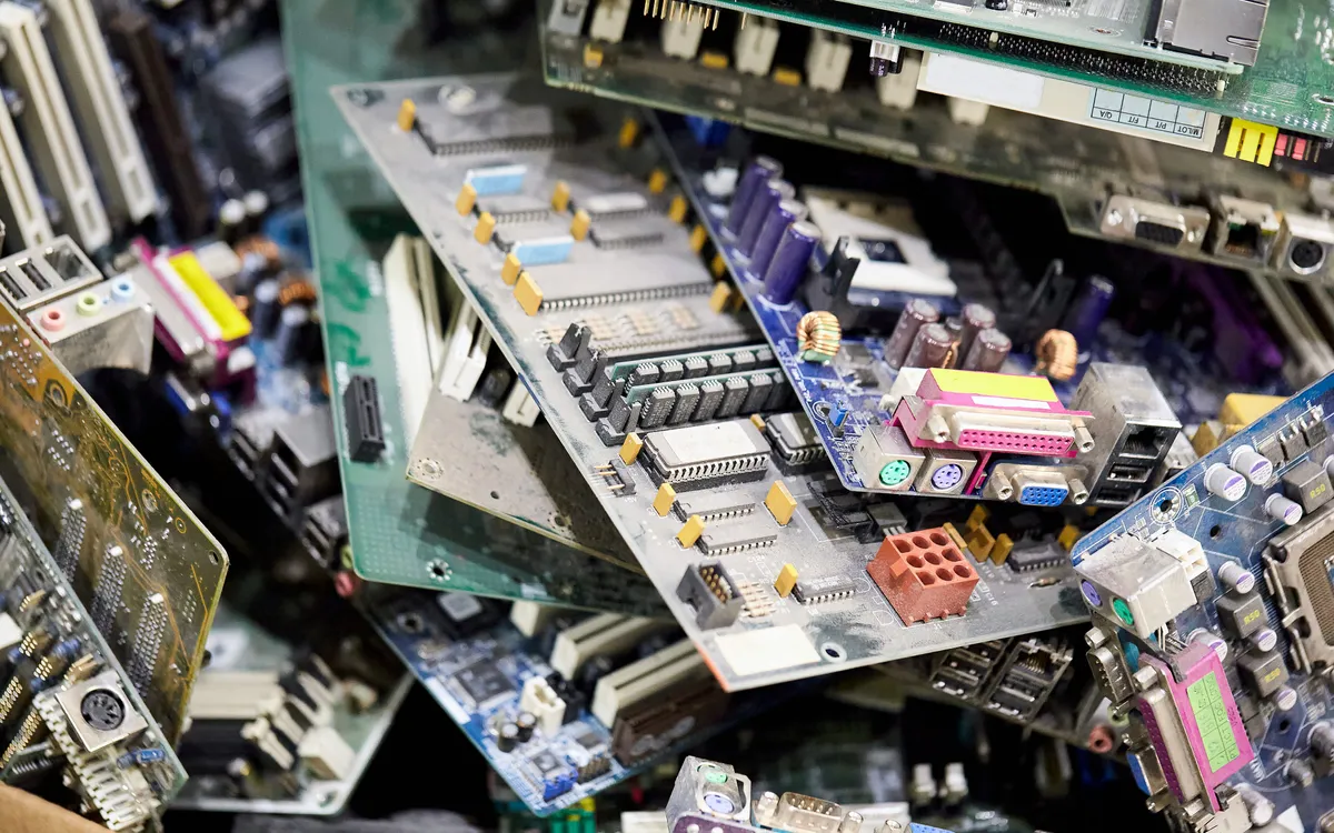
Understanding the Basics of PCB Composition
Before exploring recycling technologies, it’s important to understand what makes up a PCB. Typically, a PCB consists of:
- Non-metallic components: About 70% of a PCB is made of plastics, epoxy resins, and glass fibers, often used in the board’s substrate.
- Metallic components: Around 30% includes metals like copper (16%), tin, lead, gold, silver, and palladium. Copper is the most abundant, while precious metals like gold are present in trace amounts but hold high value.
- Hazardous materials: Small quantities of toxic substances, such as lead in solder or brominated compounds in flame retardants, require careful handling.
Separating these materials efficiently is the core challenge of PCB recycling. Traditional methods like incineration burn off non-metals but release harmful pollutants and destroy valuable resources. Advanced technologies aim to tackle this by focusing on precision and sustainability.
Advanced PCB Recycling Technologies: A Closer Look
Modern recycling methods go beyond incineration, using scientific processes to separate and recover materials with minimal environmental impact. Below, we’ll explore three key approaches: pyrometallurgy, hydrometallurgy, and electrochemical PCB recycling.
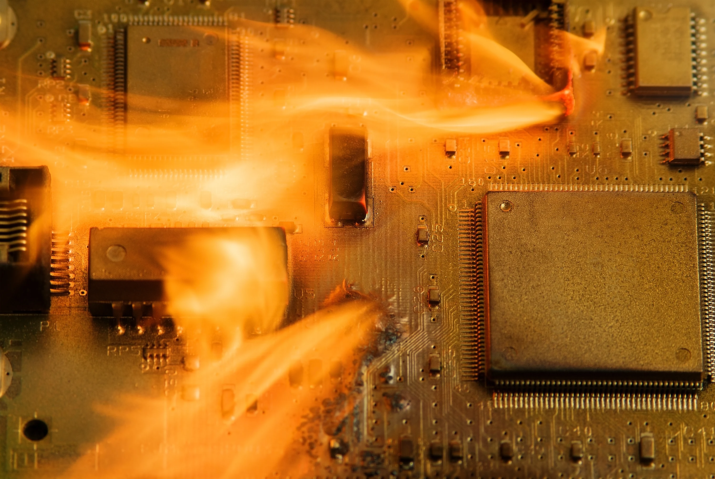
Pyrometallurgy for PCB Recycling: High-Temperature Recovery
Pyrometallurgy involves using high temperatures to extract metals from PCBs. This method is particularly effective for recovering base metals like copper and precious metals like gold and silver. Here’s how it works:
- Shredding and Pre-processing: PCBs are shredded into small pieces to increase surface area for processing.
- Smelting: The shredded material is heated in a furnace at temperatures exceeding 1200°C. This melts metals into a liquid state, separating them from non-metallic components like plastics, which burn off or turn into slag (a waste byproduct).
- Refining: The molten metals are further purified to isolate individual elements like copper, which can form alloys with tin or lead if not separated properly.
One notable technique in pyrometallurgy PCB recycling is vacuum metallurgy, which uses reduced pressure to separate metals like lead from mixed particles at lower temperatures, minimizing energy use. Studies suggest that up to 90% of copper can be recovered using this method, making it highly efficient for bulk metal extraction.
However, pyrometallurgy has drawbacks. The high energy consumption and potential emission of toxic gases (if not controlled with proper filtration) make it less ideal for complete sustainability. It’s often paired with other methods for better results.
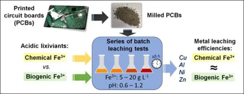
Hydrometallurgy for PCB Recycling: Chemical Leaching Solutions
Hydrometallurgy PCB recycling uses chemical solutions to dissolve and extract metals from PCBs. This method is particularly effective for recovering precious metals and is considered more environmentally friendly than pyrometallurgy. Here’s a breakdown of the process:
- Pre-treatment: PCBs are crushed into fine particles, and protective coatings are often removed using solutions like sodium hydroxide (NaOH) to expose the metals.
- Leaching: Acidic or alkaline solutions, such as hydrochloric acid (HCl) or sulfuric acid, are used to dissolve metals. For instance, HCl has shown great potential in recovering copper and gold, with recovery rates reaching up to 95% under optimal conditions.
- Separation and Recovery: Dissolved metals are separated through processes like precipitation, solvent extraction, or ion exchange, allowing individual metals to be collected in pure form.
Research indicates that increasing acid concentration and agitation speed during leaching can significantly reduce processing time. For example, a study found that using a 2M HCl solution with a shaking speed of 200 RPM can achieve near-complete metal recovery in under 4 hours. Unlike pyrometallurgy, hydrometallurgy operates at lower temperatures, reducing energy costs and emissions.
Still, challenges remain. The use of strong chemicals requires careful handling and disposal to avoid environmental contamination. Innovations in bio-hydrometallurgy, using microorganisms to leach metals, are emerging as a greener alternative, though they’re not yet widely adopted.
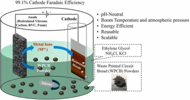
Electrochemical PCB Recycling: Precision with Electricity
Electrochemical PCB recycling is a promising technology that uses electrical currents to recover metals with high precision. This method is particularly useful for extracting valuable metals like copper and gold from complex mixtures. Here’s how it operates:
- Dissolution: Metals from shredded PCBs are dissolved into an electrolyte solution, often an acidic medium.
- Electrowinning: An electric current is applied, causing metals to deposit onto electrodes. For instance, copper can be selectively deposited at the cathode, achieving purity levels above 99%.
- Refinement: Deposited metals are collected and further processed if needed to meet industry standards.
Recent advancements have shown that electrochemical methods can recover nanoscale copper particles from PCB waste with high efficiency. A study demonstrated that combining acid leaching with low-temperature electrowinning resulted in over 90% copper recovery while minimizing energy use. This method stands out for its ability to target specific metals, reducing waste and improving material purity.
The main limitation is scalability. Electrochemical processes are often slower and more complex to set up on an industrial scale compared to pyrometallurgy or hydrometallurgy. However, ongoing research aims to optimize these systems for broader application.
Comparing the Three Methods: Which Is Best for PCB Material Separation?
Each advanced PCB recycling technology has unique strengths and weaknesses. Here’s a quick comparison to help understand their applications:
- Pyrometallurgy: Best for bulk recovery of base metals like copper. High throughput but energy-intensive and less eco-friendly without strict emission controls.
- Hydrometallurgy: Ideal for precious metal recovery with high precision. Lower energy use but involves hazardous chemicals that require safe management.
- Electrochemical: Offers the highest purity for specific metals like copper and gold. Highly sustainable but currently limited by slower processing speeds.
In practice, a hybrid approach often yields the best results. For instance, pyrometallurgy can be used for initial metal extraction, followed by hydrometallurgy or electrochemical methods for refining precious metals. This combination maximizes recovery rates—often exceeding 95% for key metals—and minimizes environmental impact.
Challenges and Future Directions in Advanced PCB Recycling
Despite the promise of these technologies, several hurdles remain. High operational costs, especially for electrochemical methods, can deter widespread adoption. Additionally, the diversity of PCB compositions makes it difficult to standardize recycling processes. A smartphone PCB, for example, may have different material ratios compared to an industrial control board, requiring tailored approaches.
Looking ahead, innovation is key. Emerging technologies like bio-leaching (using bacteria for metal extraction) and solvent-based separation are gaining traction for their low environmental impact. Governments and industries are also pushing for stricter e-waste regulations, encouraging investment in sustainable recycling infrastructure. By 2030, it’s estimated that the global e-waste recycling market could exceed $50 billion, driven by advancements in PCB material separation techniques.
The Role of Design in Facilitating PCB Recycling
While recycling technologies are crucial, PCB design plays a significant role in making recycling easier. Designers can prioritize eco-friendly materials, reduce the use of hazardous substances, and create modular boards that are simpler to disassemble. For instance, using lead-free solder not only complies with regulations like RoHS (Restriction of Hazardous Substances) but also simplifies metal separation during recycling.
Manufacturers can also label components with material information to streamline sorting processes. By integrating recyclability into the design phase, the industry can create a circular economy where materials are reused rather than discarded.
Conclusion: Building a Sustainable Future with Advanced PCB Recycling
The shift from incineration to advanced PCB recycling technologies marks a significant step toward sustainability. Methods like pyrometallurgy, hydrometallurgy, and electrochemical PCB recycling offer efficient ways to recover valuable materials while minimizing environmental harm. Though challenges like cost and scalability persist, ongoing research and industry collaboration are paving the way for greener solutions.
By embracing these innovations and focusing on recyclable designs, we can tackle the growing e-waste crisis and conserve resources for future generations. Whether you’re an engineer, manufacturer, or environmental advocate, understanding and supporting advanced PCB material separation is key to creating a cleaner, more sustainable world.


