 ALLPCB


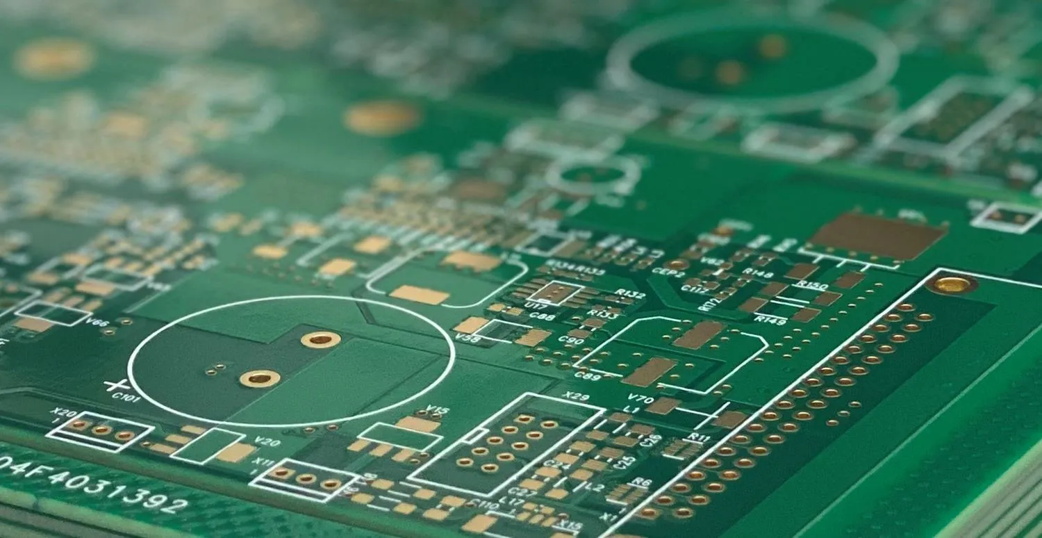
If you're new to PCB design and manufacturing, you might be wondering, "What is a solder mask, and why is it important?" A solder mask is a thin protective layer applied to a printed circuit board (PCB) to cover copper traces, preventing oxidation and accidental solder bridges during assembly. It’s essential for ensuring the reliability and functionality of your PCB by protecting the board and guiding solder to the right spots. In this comprehensive guide, we’ll dive into why you should use a solder mask, the different types available, popular solder mask colors, and how they are made, providing you with all the basics to understand this critical PCB component.
What Is a Solder Mask?
A solder mask, also known as solder resist or solder stop, is a polymer layer applied to the surface of a PCB. This thin coating covers the copper traces and pads, leaving only the areas meant for soldering exposed. Think of it as a protective shield for your board. It prevents environmental damage, such as oxidation, and ensures that solder sticks only to the intended spots during the assembly process.
Without a solder mask, the copper on a PCB can corrode over time due to exposure to air and moisture. Additionally, during soldering—especially in automated processes like reflow or wave soldering—solder could accidentally connect two nearby pads, creating a short circuit known as a solder bridge. The solder mask acts as a barrier to stop this from happening, making it a must-have for most modern PCBs, especially those produced in large quantities.
Why Use a Solder Mask?
Using a solder mask on your PCB offers several key benefits that make it indispensable in manufacturing. Let’s break down the main reasons why it’s so widely used:
- Protection Against Oxidation: Copper traces on a PCB are prone to oxidation when exposed to air. Oxidation can degrade the conductivity of the traces, leading to poor performance or failure. A solder mask forms a barrier that shields the copper from environmental factors, extending the lifespan of the board.
- Prevention of Solder Bridges: During soldering, especially in high-density designs with closely spaced pads, solder can unintentionally flow between pads, creating unwanted electrical connections. The solder mask isolates these areas, ensuring solder only adheres to the designated spots.
- Improved Insulation: The solder mask acts as an insulating layer, reducing the risk of electrical shorts caused by dust, debris, or accidental contact with conductive materials during handling or operation.
- Enhanced Durability: PCBs often face harsh conditions, including temperature changes and humidity. A solder mask adds an extra layer of durability, protecting the board from physical and environmental stress.
- Better Aesthetics and Labeling: Beyond functionality, solder masks give PCBs a polished, professional look. They also provide a surface for silkscreen printing, which is used to add labels, component identifiers, and other markings for easier assembly and troubleshooting.
In short, a solder mask is critical for both the performance and longevity of a PCB. While it’s sometimes skipped in simple, hand-soldered prototypes, it’s a standard feature in professional and mass-produced boards due to its protective and practical advantages.
Different Types of Solder Mask
Not all solder masks are the same. There are several types available, each suited to different applications and manufacturing processes. Understanding these options can help you choose the right one for your project. Here are the main types of solder mask materials used in PCB production:
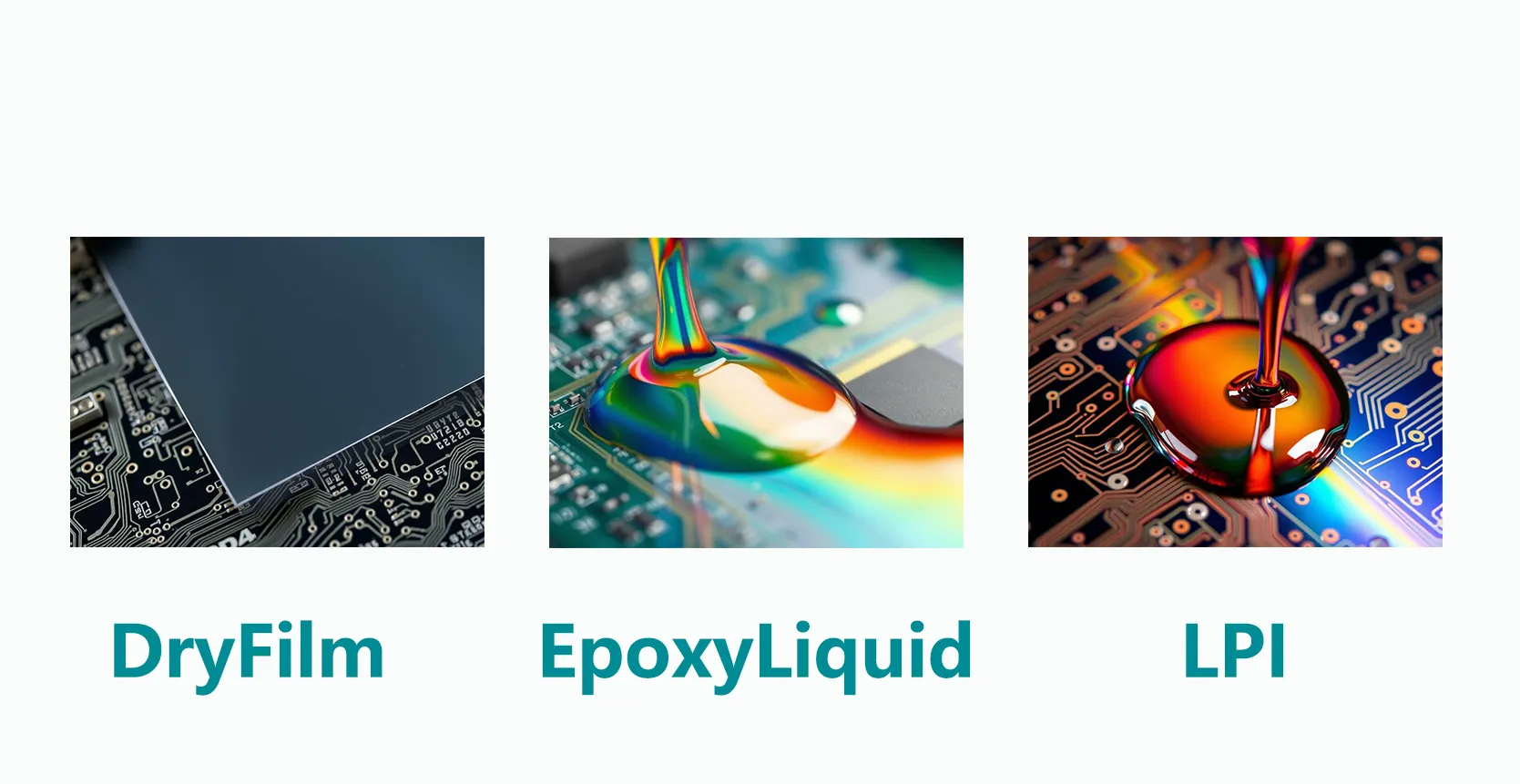
1. Epoxy Liquid Solder Mask
This is one of the most common and cost-effective types of solder mask. Epoxy liquid is applied to the PCB using a screen-printing process and then cured with heat. It’s ideal for less complex designs because it offers decent protection at a lower cost. However, it may not provide the precision needed for high-density or fine-pitch components due to potential inconsistencies in thickness.
2. Liquid Photoimageable Solder Mask (LPI)
Liquid Photoimageable (LPI) solder mask is a more advanced option widely used in modern PCB manufacturing. It’s applied as a liquid coating across the entire board, then exposed to UV light through a photomask to define the areas that remain. The unexposed areas are washed away, leaving precise openings for soldering. LPI is highly accurate, making it perfect for intricate designs with tight tolerances, such as those with surface-mount components. It’s also more durable than epoxy liquid masks.
3. Dry Film Photoimageable Solder Mask
Dry film solder mask comes as a solid sheet that’s laminated onto the PCB surface under heat and pressure. Like LPI, it’s processed using UV light and a photomask to create precise openings. This type is often used for high-resolution applications because it offers uniform thickness and excellent adhesion. However, it can be more expensive and complex to apply compared to liquid options.
4. Top and Bottom Side Masks
While not a material type, it’s worth noting that solder masks are typically applied to both the top and bottom sides of a PCB. Each side can have different requirements based on the components and layout. Some designs might even use different mask types or colors on each side for functional or aesthetic reasons.
Choosing the right type of solder mask depends on factors like your budget, the complexity of your PCB design, and the manufacturing capabilities available. For most beginners, starting with LPI is a safe bet due to its balance of precision and cost.
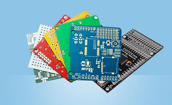
Popular Solder Mask Colors
When you think of a PCB, you probably picture a green board. Green is the traditional and most common solder mask color, but it’s not the only option. Solder mask colors can vary, and each has its own practical and aesthetic purposes. Let’s explore the most popular choices and why they’re used:
1. Green
Green is the standard solder mask color and has been for decades. It’s widely used because it offers good contrast with the white silkscreen labels, making text and markings easy to read. Green also helps during visual inspections, as defects like scratches or misalignments stand out against the color. Additionally, it’s often the most cost-effective option due to its widespread use and compatibility with manufacturing processes.
2. Red
Red solder masks are often chosen for aesthetic reasons, giving a bold and striking look to the PCB. They’re popular in consumer electronics or prototypes where appearance matters. However, red can make it harder to spot defects compared to green, and silkscreen text might not contrast as well unless yellow or another light color is used.
3. Blue
Blue solder masks are another visually appealing option, often used in branded products or designs where a unique look is desired. Like red, blue may reduce visibility for inspections but can be paired with white or yellow silkscreen for better readability.
4. Black
Black solder masks are less common but are used for specific applications, such as in LED displays or optical devices, because they minimize light reflection. However, black can absorb heat, which might affect performance in high-temperature environments. It also makes visual inspections challenging unless paired with bright silkscreen colors.
5. White
White solder masks are rare but useful in applications like LED lighting, where they help reflect light for better efficiency. They’re harder to keep clean and show dirt or defects more easily, so they’re not ideal for all projects.
6. Yellow and Other Custom Colors
Yellow and other less common colors are sometimes used for specialized or custom designs. These colors often come at a higher cost and may not be as compatible with standard manufacturing processes, so they’re typically reserved for specific branding or functional needs.
While color choice might seem like a small detail, it can impact both the functionality and appearance of your PCB. For beginners, sticking with green is usually the safest and most practical choice unless your project has specific requirements.
How Solder Masks Are Made and Applied
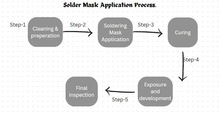
Understanding how solder masks are made and applied can give you insight into the PCB manufacturing process. While the exact method depends on the type of solder mask being used, the general steps are similar. Here’s a simplified overview of how solder masks are created and added to a PCB:
Step 1: Preparation of the PCB
Before applying the solder mask, the PCB surface must be clean and free of contaminants. Any dust, oil, or residue on the copper traces can prevent proper adhesion of the mask. The board is thoroughly cleaned, often using chemical solutions or abrasive methods, to ensure a smooth surface.
Step 2: Application of the Solder Mask Material
The method of application varies based on the type of solder mask:
- Epoxy Liquid: This is applied using a screen-printing technique, where the liquid mask is pushed through a mesh screen onto the PCB, covering the desired areas. It’s a relatively simple and low-cost method but less precise.
- Liquid Photoimageable (LPI): The liquid is sprayed or rolled onto the entire PCB surface as a thin, even layer. This method allows for better control over thickness and coverage.
- Dry Film: A solid sheet of solder mask material is laminated onto the PCB using heat and pressure. This ensures a uniform thickness but requires more specialized equipment.
Step 3: Defining the Pattern (For Photoimageable Masks)
For LPI and dry film masks, the next step is to define where the mask will remain and where it will be removed to expose copper for soldering. A photomask—a film with the desired pattern—is placed over the board, and the setup is exposed to UV light. The light hardens the solder mask in the areas that will stay, while unexposed areas remain soft and are later washed away with a developer solution. This creates precise openings for pads and vias.
Step 4: Curing the Solder Mask
Once the mask is applied and patterned, it needs to be cured to harden and bond permanently to the PCB. This is typically done using heat (thermal curing) or additional UV exposure, depending on the material. Curing ensures the mask can withstand the soldering process and environmental stress.
Step 5: Inspection and Quality Control
After curing, the PCB is inspected to ensure the solder mask is applied correctly. Manufacturers check for issues like incomplete coverage, misalignment, or defects in the openings. Advanced techniques, such as automated optical inspection (AOI), are often used to verify quality, especially for high-volume production.
The entire process is carefully controlled to meet industry standards, ensuring the solder mask performs its protective and insulating functions. For beginners, it’s helpful to know that this step is handled by the manufacturer, but you’ll need to provide accurate design files with clear solder mask layers to avoid errors.
Tips for Beginners When Working with Solder Masks
If you’re just starting with PCB design, here are a few practical tips to keep in mind regarding solder masks:
- Include Solder Mask Layers in Your Design Files: When submitting your PCB design for manufacturing, ensure your Gerber files include clearly defined solder mask layers. This tells the manufacturer exactly where to apply the mask and where to leave openings for soldering.
- Consider Solder Mask Clearance: Design with enough clearance around pads (often 0.1 mm or more, depending on the manufacturer’s capabilities) to avoid overlap or misalignment issues during application.
- Stick to Standard Colors for Cost Efficiency: Unless your project requires a specific color for branding or functionality, choose green to keep costs down and ensure compatibility with standard processes.
- Double-Check Design Rules: Use your design software’s design rule check (DRC) to ensure your solder mask aligns with the copper layers and meets manufacturing tolerances. Errors here can lead to exposed traces or covered pads.
- Communicate with Your Manufacturer: If you’re unsure about solder mask options or requirements, reach out to your manufacturing partner for guidance. They can advise on the best type and color for your specific project.
Common Solder Mask Issues and How to Avoid Them
Even with careful planning, solder mask issues can arise during manufacturing. Being aware of these problems can help you design better PCBs. Here are a few common issues and how to prevent them:
- Solder Mask Misalignment: If the mask isn’t aligned properly with the copper pads, it can cover areas meant for soldering or leave traces exposed. To avoid this, ensure your design files are accurate and adhere to the manufacturer’s minimum clearance and tolerance specifications.
- Incomplete Coverage: Sometimes, the mask might not fully cover the intended areas due to application errors or surface contamination. Work with a reliable manufacturer who follows strict quality control processes to minimize this risk.
- Peeling or Delamination: Poor adhesion can cause the solder mask to peel off over time, especially under harsh conditions. This can be prevented by ensuring proper surface preparation and curing during manufacturing.
- Color Inconsistencies: If aesthetics are important, note that custom colors might vary slightly between batches. Stick to standard colors if consistency is critical, or discuss expectations with your manufacturer.

Conclusion
A solder mask is a small but vital part of any PCB, offering protection, insulation, and precision during soldering. For beginners, understanding what a solder mask is, why it’s used, the different types available, popular colors, and how it’s made can make a big difference in designing reliable and professional boards. Whether you’re working on a simple prototype or preparing for mass production, paying attention to solder mask details ensures your PCB performs as intended and lasts longer.
By following the tips and insights shared in this guide, you’re well on your way to mastering the basics of solder masks. As you gain experience, you’ll learn how to tailor your choices—whether it’s the type of mask or the color—to suit your specific projects. With this knowledge, you can confidently design PCBs that meet both functional and aesthetic goals.


