 ALLPCB


In the world of printed circuit board (PCB) manufacturing, one hidden issue can cause major problems: copper imbalance. This often-overlooked factor is a leading cause of PCB warpage, resulting in manufacturing defects, assembly issues, and even complete board failure. If you're dealing with warped boards or aiming to prevent PCB bending, understanding copper distribution in PCBs and applying proper balancing techniques is critical. In this detailed guide, we'll explore the causes of PCB warpage, the role of copper imbalance, and practical strategies to ensure your boards remain flat and functional.
What Is PCB Warpage and Why Does It Matter?
PCB warpage refers to the bending or twisting of a printed circuit board, causing it to deviate from its intended flat shape. This defect can occur during manufacturing, soldering, or even after PCB assembly. Warped boards create a host of problems, such as misaligned components, poor solder joints, and mechanical stress that can lead to cracks or failures. In severe cases, warpage can render a board unusable, increasing production costs and delaying projects.
The impact of warpage is especially significant in high-density designs or applications requiring precision, such as aerospace, automotive, or medical devices. For instance, a warped PCB in a surface-mount technology (SMT) assembly line can lead to defects like tombstoning, where components stand upright due to uneven soldering. Preventing PCB warpage is not just about aesthetics—it's about ensuring reliability and performance.
Key Causes of PCB Warpage: Why Copper Imbalance Is a Silent Killer
Warpage in PCBs can stem from several factors, but copper imbalance stands out as a primary and often silent culprit. Let's break down the main causes of PCB warpage, focusing on how uneven copper distribution plays a critical role.
1. Uneven Copper Distribution Across Layers
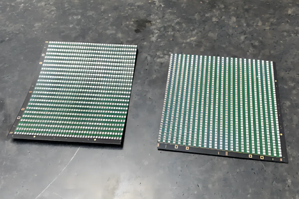
PCBs are made of multiple layers, often with copper traces and planes distributed across them. When the copper density varies significantly between layers or even within the same layer, it creates uneven thermal expansion during manufacturing processes like lamination or reflow soldering. For example, a layer with a large copper plane on one side and minimal copper on the other will expand and contract at different rates when exposed to heat, leading to bending.
In numbers, copper has a coefficient of thermal expansion (CTE) of about 17 ppm/°C, while the base material (like FR-4) has a CTE of around 14-16 ppm/°C in the X-Y direction. This slight mismatch, combined with uneven copper, amplifies stress and warpage during temperature changes, such as the 260°C peak in reflow ovens.
2. Thermal Stress During Manufacturing
High temperatures in processes like lamination, soldering, or curing can exacerbate warpage if copper distribution isn't balanced. As the board heats up and cools down, areas with more copper retain heat longer, causing uneven shrinkage. This is especially problematic in multilayer boards where inner layers may have different copper densities.
3. Material Mismatch and Design Flaws
Beyond copper, the choice of materials and design practices can contribute to warpage. Using substrates with mismatched CTEs or stacking layers improperly can create internal stresses. However, copper imbalance often compounds these issues, making it a critical factor to address.
Suggested Reading:What Causes PCB Warpage?
How Copper Imbalance Directly Leads to PCB Manufacturing Defects
Copper imbalance doesn't just cause warpage—it triggers a cascade of manufacturing defects that can compromise the entire board. Here's how this silent killer impacts PCB production:
- Poor Solder Joints: Warped boards prevent components from sitting flat, leading to uneven solder paste application. This can result in weak joints or open circuits, especially in fine-pitch components where precision is key.
- Component Misalignment: During SMT assembly, a non-flat PCB can cause components to shift, leading to misalignment. This often requires costly rework or scrapping of the board.
- Mechanical Stress and Cracks: Warpage introduces stress points that can cause micro-cracks in traces or vias, reducing the board's lifespan. In high-reliability applications, this is a major concern.
- Signal Integrity Issues: For high-speed designs, warpage can alter trace impedance (typically targeted at 50 ohms for many applications). Even a small deviation can lead to signal loss or crosstalk.
These defects highlight why copper distribution in PCBs is not just a design detail—it's a make-or-break factor for quality and reliability.
PCB Copper Balancing Techniques to Prevent Warpage
Now that we understand the role of copper imbalance in PCB warpage, let's dive into actionable techniques to achieve proper copper distribution and prevent bending. These strategies are practical for engineers and designers at any stage of the PCB process.
1. Design for Symmetry in Copper Distribution
One of the most effective ways to prevent PCB warpage is to design for symmetry. This means ensuring that copper density is roughly equal on both sides of the board and across corresponding layers in multilayer designs. For instance, if one layer has a large ground plane, mirror a similar plane on the opposite layer to balance thermal expansion.
In practice, aim for a copper coverage difference of no more than 10-15% between opposing layers. Many design tools allow you to calculate copper density during the layout phase, making it easier to spot and correct imbalances early.
2. Use Copper Thieving or Dummy Patterns
Copper thieving involves adding non-functional copper shapes or patterns to areas with low copper density. These "dummy" fills balance the overall copper distribution without affecting the board's electrical performance. Place these patterns in open areas of the PCB, ensuring they don't interfere with signal traces or vias.
This technique is especially useful for boards with sparse trace layouts on one side. By filling empty spaces, you reduce the risk of uneven thermal stress during manufacturing.
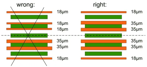
3. Optimize Layer Stack-Up for Balance
In multilayer PCBs, the stack-up design plays a huge role in preventing warpage. Arrange layers so that copper planes and trace densities are symmetrically distributed around the board's centerline. For example, in a 4-layer board, ensure that layers 1 and 4 (outer layers) and layers 2 and 3 (inner layers) have similar copper coverage.
Additionally, consult with your manufacturer about material choices. Some substrates are more prone to warpage under thermal stress, so selecting a material with a CTE closer to copper can minimize risks.
4. Control Manufacturing Parameters
While design is critical, manufacturing processes also influence warpage. Work with your fabrication partner to control lamination pressures and temperatures. For instance, excessive pressure during lamination can lock in stresses caused by copper imbalance, while uneven cooling after reflow can worsen bending. Ensure cooling is gradual and uniform to avoid thermal shocks.
5. Simulate and Test Designs Before Production
Before sending your design for fabrication, use simulation tools to predict potential warpage. Many PCB design software platforms offer thermal and mechanical analysis features that can highlight areas of copper imbalance. Testing prototypes under real-world conditions, such as reflow soldering at 260°C, can also reveal warpage risks early on.
Best Practices to Prevent PCB Bending Beyond Copper Balance
While copper balancing is crucial, a holistic approach to PCB design and manufacturing can further reduce the risk of warpage. Here are additional best practices to keep your boards flat and functional:
- Choose the Right Board Thickness: Thinner boards (e.g., below 0.8 mm) are more prone to bending. Opt for a thickness that provides structural stability, especially for larger PCBs.
- Avoid Large Unsupported Areas: Large areas without components or copper can flex more easily. Reinforce these zones with dummy fills or mechanical supports.
- Minimize Thermal Cycles: Repeated exposure to high temperatures during assembly or rework can increase warpage. Optimize your process to reduce thermal stress.
- Store Boards Properly: Improper storage, such as stacking boards unevenly or exposing them to humidity, can induce warpage before assembly. Store PCBs flat in a controlled environment.
Suggested Reading:Large PCB Panel (≥500mm) Warpage Control
Why Preventing PCB Warpage Saves Time and Money
Investing effort in copper balancing and warpage prevention isn't just about technical perfection—it's a smart business decision. Warped boards lead to higher scrap rates, increased rework costs, and delays in production. For example, a single batch of defective PCBs can cost thousands of dollars in materials and labor, not to mention the potential loss of customer trust if faulty products reach the market.
By applying the techniques discussed, such as symmetrical copper distribution and optimized stack-ups, you can achieve higher yields and faster time-to-market. In industries where reliability is non-negotiable, preventing PCB bending also ensures compliance with strict quality standards.
Conclusion: Take Control of Copper Imbalance for Flawless PCBs
PCB warpage, driven by copper imbalance, is a silent killer that can undermine even the most carefully designed boards. By understanding the causes of warpage—such as uneven copper distribution and thermal stress—you can take proactive steps to prevent bending and other manufacturing defects. Techniques like designing for symmetry, using copper thieving, and optimizing layer stack-ups are powerful tools to achieve balanced copper distribution in PCBs.


