ALLPCB


If you're new to PCB manufacturing or quality control, you might be wondering how to ensure the hidden components and connections in your printed circuit boards (PCBs) are free from defects. PCB X-ray inspection is a powerful tool that allows you to see beneath the surface of a board, identifying issues that are invisible to the naked eye. In this step-by-step guide, we'll walk you through the basics of PCB X-ray inspection, from understanding how it works to setting up equipment and interpreting images for defect identification. Whether you're searching for a PCB X-ray inspection tutorial or want to master X-ray basics, this blog will provide actionable insights to help you get started.
What Is PCB X-ray Inspection and Why Does It Matter?
PCB X-ray inspection is a non-destructive testing method used to examine the internal structure of a printed circuit board. Unlike visual inspections or automated optical inspection (AOI), which only assess the surface, X-ray technology penetrates the board to reveal hidden defects like solder voids, misaligned components, or broken connections. This is especially critical for modern PCBs with complex designs, such as those with ball grid arrays (BGAs) or multi-layer structures, where issues can hide beneath components or within layers.
The importance of X-ray inspection lies in its ability to improve product reliability. For example, a single solder void in a BGA can lead to a failure rate of up to 10% in high-stress applications, according to industry studies. By catching these defects early, manufacturers can reduce costly rework and ensure their products meet strict quality standards. This PCB X-ray inspection tutorial will break down the process so beginners can understand its value and application.
X-ray Basics: How Does PCB X-ray Inspection Work?
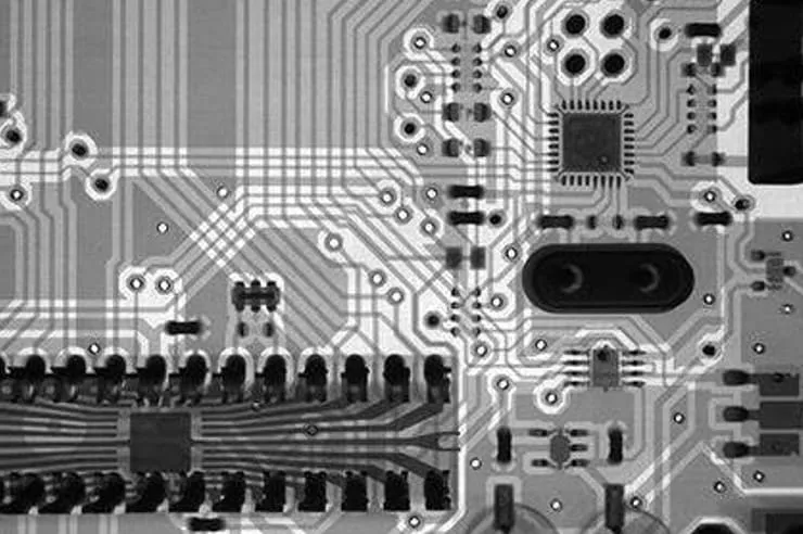
Before diving into the practical steps, let’s cover the fundamentals of X-ray technology for PCB inspection. X-rays are a form of electromagnetic radiation with a wavelength short enough to pass through materials like plastic, epoxy, and even thin metal layers. When X-rays hit a PCB, denser materials (like copper traces or solder) absorb more radiation and appear darker in the resulting image, while less dense areas (like air gaps or voids) appear lighter.
The core components of an X-ray inspection system include:
- X-ray Source: Generates the radiation that passes through the PCB.
- Detector: Captures the X-rays after they pass through the board, converting them into a digital image.
- Sample Stage: Holds the PCB in place and may rotate or tilt for multi-angle views.
- Software: Processes the images and allows for analysis and defect identification.
Understanding these X-ray basics is essential for beginners because they form the foundation of how you’ll set up and use the equipment. The process is safe when proper precautions are taken, as modern systems are designed with shielding to minimize radiation exposure.
Step 1: Equipment Setup for PCB X-ray Inspection
Setting up an X-ray inspection system might seem daunting, but with the right approach, it’s manageable even for beginners. Here’s how to prepare your equipment for effective PCB inspection:
- Choose the Right System: Select an X-ray machine suited for PCB inspection. Look for systems with a voltage range of 80-160 kV, as this range is ideal for penetrating typical PCB materials without overexposure. Higher voltage might be needed for thicker boards or dense components.
- Position the PCB: Place the board on the sample stage, ensuring it’s flat and secure. If inspecting a specific area, align it directly under the X-ray source for the clearest image.
- Adjust Settings: Set the voltage and current based on the PCB’s thickness and material. For a standard 1.6mm FR4 board, start with 100 kV and 0.1 mA, then adjust as needed for image clarity.
- Calibrate the Detector: Ensure the detector is properly aligned with the source to avoid distorted images. Most modern systems have automated calibration features, but double-check the setup.
- Safety First: Verify that all shielding is in place and that operators are wearing protective gear if required. Follow local regulations for radiation safety.
Proper equipment setup is a critical part of this PCB X-ray inspection tutorial because it ensures accurate results. A poorly configured system can lead to unclear images, making defect identification nearly impossible.
Step 2: Capturing X-ray Images of Your PCB
Once your equipment is ready, the next step is to capture high-quality X-ray images. Follow these guidelines to ensure usable results:
- Start with a Test Run: Take a low-resolution image first to check alignment and settings. Adjust the position or parameters if the image is too dark or blurry.
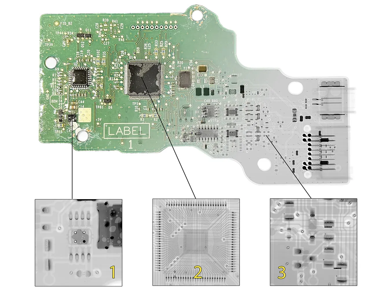
- Use Multiple Angles: For complex PCBs, capture images from different angles (e.g., top-down and 45-degree oblique views) to see hidden defects in 3D components like BGAs.
- Optimize Exposure Time: Keep exposure between 1-5 seconds for most PCBs. Longer exposure can improve detail but may cause image noise if overdone.
- Save and Label Images: Store images in a high-resolution format (like TIFF) and label them with the PCB batch number and inspection date for traceability.
Capturing clear images is the backbone of effective image interpretation, which we’ll cover next. If your images are poor quality, even the best analysis software won’t help.
Step 3: Image Interpretation for Beginners
Interpreting X-ray images is where the real work of PCB inspection begins. As a beginner, focus on understanding the contrast and shapes in the image to spot potential issues. Here’s how to approach image interpretation:
- Understand Contrast: Dark areas represent dense materials like solder or copper, while light areas indicate gaps, air, or less dense materials. A bright spot in a solder joint, for instance, might indicate a void.
- Look for Patterns: Familiarize yourself with how a defect-free PCB looks under X-ray. For example, a BGA should show a uniform grid of dark solder balls. Deviations from this pattern could signal misalignment or missing connections.
- Use Software Tools: Many X-ray systems come with software that enhances images or highlights anomalies. Use zoom and contrast adjustment features to examine small details.
- Compare with Standards: Refer to industry standards like IPC-A-610 for acceptable defect levels. For instance, solder voids larger than 25% of the joint area are often considered unacceptable.
Image interpretation takes practice, but over time, you’ll develop an eye for spotting irregularities. This skill is crucial for defect identification, which we’ll dive into next as part of this PCB X-ray inspection tutorial.
Step 4: Defect Identification in PCB X-ray Images
Identifying defects is the ultimate goal of X-ray inspection. Here are some common issues to look for and how they appear in X-ray images:
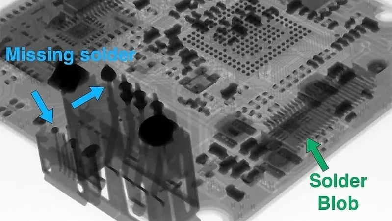
- Solder Voids: Appear as light spots within dark solder joints. Voids larger than 20-25% of the joint area can weaken the connection, increasing the risk of failure under thermal stress.
- Broken Traces: Show as gaps in the dark lines of copper traces. Even a small break can disrupt signal integrity, leading to circuit failure.
- Misaligned Components: Visible as components that don’t align with their solder pads. For BGAs, look for solder balls that are offset from the grid pattern.
- Insufficient Solder: Appears as thinner or less dense dark areas in joints. This can cause poor electrical conductivity, with resistance values potentially rising above 0.1 ohms in affected areas.
- Bridging: Looks like dark lines connecting adjacent solder points. This can cause short circuits, especially in high-density designs.
Document any defects you find, noting their location and severity. This data helps in deciding whether a board needs rework or can be passed for assembly. Defect identification is a skill that improves with experience, so start with simple boards and gradually move to more complex designs.
Suggested Reading: The Ultimate Guide to PCB X-ray Inspection: Ensuring Quality and Reliability
Benefits of PCB X-ray Inspection for Quality Control
Now that you understand the process, let’s highlight why PCB X-ray inspection is a game-changer for quality control. First, it catches defects that other methods miss. For instance, AOI can’t detect internal solder issues, but X-ray inspection reveals them with up to 95% accuracy in controlled tests. Second, it’s non-destructive, meaning you don’t have to damage the board to inspect it. Finally, it saves time and money by identifying issues early—rework costs can be reduced by 30-50% when defects are caught before final assembly.
For beginners, adopting X-ray inspection as part of your workflow ensures that your products meet high reliability standards, especially in industries like automotive or aerospace where failure rates must be below 0.01%.
Common Challenges and Tips for Beginners
As with any new skill, PCB X-ray inspection comes with challenges. Here are a few common hurdles and how to overcome them:
- Blurry Images: Often caused by incorrect settings or movement during capture. Double-check voltage and exposure time, and ensure the PCB is secure.
- Misinterpreting Defects: Beginners might confuse normal variations for defects. Cross-reference images with known good samples to build confidence.
- Equipment Cost: High-end X-ray systems can be expensive, but many service providers offer inspection as a contracted service, saving upfront investment.
- Safety Concerns: Always follow safety protocols and ensure proper training for anyone operating the equipment.
Patience and practice are key. Start small, focus on mastering the basics, and gradually tackle more complex inspections as you gain experience.
Conclusion: Mastering PCB X-ray Inspection as a Beginner
PCB X-ray inspection is an invaluable tool for ensuring the quality and reliability of printed circuit boards, especially as designs become more intricate. By following this step-by-step guide, you’ve learned the essentials of X-ray basics, equipment setup, image capture, image interpretation, and defect identification. This PCB X-ray inspection tutorial is designed to help beginners build a strong foundation, paving the way for more advanced applications in quality control.
Implementing X-ray inspection in your process can significantly reduce failure rates and improve product performance. With practice, you’ll gain the confidence to spot even the smallest defects, ensuring your PCBs meet the highest standards. Keep learning, stay consistent, and leverage this powerful technology to elevate your manufacturing process.