ALLPCB


If you're wondering how V-scoring affects PCB signal integrity, the answer lies in its minimal direct impact but significant indirect influence. V-scoring, a method used to create grooves for easy separation of PCBs from a panel, can indirectly affect signal integrity by influencing component placement, trace routing, and potential mechanical stress near the scored areas. In this comprehensive guide, we'll dive deep into the relationship between V-scoring, PCB impedance, and signal performance, providing actionable insights for engineers looking to optimize their designs for both manufacturability and reliability.
What is V-Scoring in PCB Manufacturing?
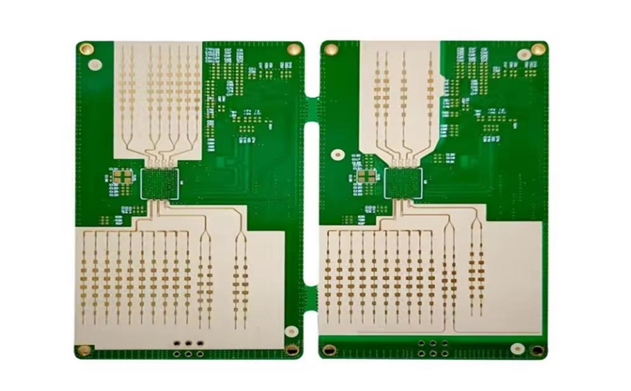
V-scoring is a technique used in PCB manufacturing to facilitate the separation of individual boards from a larger panel. By cutting V-shaped grooves into both sides of the panel, it creates a weakened line that allows the boards to be snapped apart easily after assembly. This method is widely favored for its efficiency, especially in high-volume production, as it reduces the need for additional tools or complex separation processes.
While V-scoring is primarily a mechanical process, its placement and execution can have subtle effects on the electrical performance of a PCB. Understanding these effects is crucial for maintaining signal integrity, especially in high-speed or high-frequency designs where even small disruptions can lead to significant issues.
Understanding Signal Integrity in PCBs
Signal integrity refers to the quality and reliability of electrical signals as they travel through a PCB. Factors like impedance mismatches, crosstalk, reflections, and noise can degrade signal integrity, leading to data errors or system failures. In modern electronics, where speeds can exceed several gigahertz, maintaining signal integrity is a top priority for engineers.
Key elements affecting signal integrity include:
- PCB Impedance: The resistance to signal flow, which must be controlled to match the source and load for minimal reflection. Typical controlled impedance values for high-speed designs range from 50 to 100 ohms.
- Trace Routing: The layout of conductive paths must avoid sharp bends or unnecessary length to prevent signal delay or interference.
- Material Properties: The dielectric constant of the PCB substrate affects signal speed, often ranging from 3.5 to 4.5 for common materials like FR-4.
- External Stress: Mechanical stress or environmental factors can alter trace geometry or material properties, impacting performance.
V-scoring intersects with signal integrity primarily through mechanical stress and layout constraints, which we’ll explore in detail below.
How V-Scoring Affects PCB Signal Integrity
While V-scoring itself does not directly interact with electrical signals, its implementation can influence design decisions and manufacturing outcomes that do affect signal integrity. Let’s break down the key areas of impact.
1. Component Placement and Keep-Out Zones
V-scoring requires a certain amount of space along the edges of individual PCBs within a panel. To prevent damage during separation, components and traces are typically kept away from these scored areas, creating "keep-out zones." For high-speed designs, this can limit the available space for critical signal traces, potentially forcing longer or less optimal routing paths.
For example, if a differential pair needs to maintain a specific length and spacing for impedance control (often around 50 ohms for USB or HDMI signals), a keep-out zone near a V-score line might necessitate a detour. This detour could introduce signal delay or increase the risk of crosstalk with nearby traces.
Tip for Engineers: Plan your layout with V-scoring in mind from the start. Ensure critical high-speed traces are routed away from panel edges, and use simulation tools to verify impedance and signal timing after layout adjustments.
2. Mechanical Stress and Micro-Cracks
The process of snapping a PCB along a V-scored line introduces mechanical stress to the board. If not done carefully, this can lead to micro-cracks or delamination near the scored area. These physical defects can alter the dielectric properties of the PCB material or even damage nearby traces, leading to impedance mismatches or signal loss.
For instance, a micro-crack in the substrate could change the effective dielectric constant near a trace, shifting the impedance from a target of 50 ohms to an undesirable value like 55 ohms. Even a 5% deviation can cause noticeable signal reflections in high-speed applications operating at frequencies above 1 GHz.
Tip for Engineers: Specify precise V-scoring depth and angle in your design files (typically a depth of 1/3 the board thickness on each side). Work closely with your manufacturer to ensure clean separation processes that minimize stress on the board.
3. Panelization Constraints on High-Speed Designs
In panelized designs, V-scoring dictates how multiple PCBs are arranged and separated. For high-speed or RF designs, the orientation of boards within a panel can affect signal integrity if sensitive traces are placed near panel edges or if grounding planes are disrupted by scoring lines. Poor panelization might also require additional vias or connectors for testing, which can introduce parasitic inductance or capacitance, further degrading signals.
As an example, consider a 5G application where signal speeds reach 10 Gbps. Any added inductance from vias near a V-score line could cause a measurable increase in signal jitter, reducing system reliability.
Tip for Engineers: Optimize panelization to keep high-speed signals away from V-scoring edges. Use ground planes strategically to shield sensitive areas, and minimize vias near separation lines.
V-Scoring and PCB Impedance: A Closer Look
PCB impedance is a critical factor in signal integrity, especially for high-speed digital and RF circuits. While V-scoring doesn’t directly alter impedance, its influence on trace routing and mechanical integrity can create indirect effects.
For instance, if a trace must be rerouted around a V-scoring keep-out zone, the change in length or proximity to other traces could disrupt the controlled impedance. A standard single-ended trace designed for 50 ohms might shift to 52 or 48 ohms due to altered spacing or dielectric thickness near the scored edge. Even small changes like this can lead to signal reflections, especially at frequencies above 500 MHz.
Additionally, mechanical stress from V-scoring separation could cause subtle deformations in the PCB substrate, affecting the dielectric constant and, consequently, the impedance. For high-precision designs, such as those in telecommunications or aerospace, these variations must be accounted for during simulation and testing.
Tip for Engineers: Use impedance calculators and field solvers during the design phase to predict and mitigate any deviations caused by layout constraints near V-scoring lines. Post-manufacturing testing with a Time Domain Reflectometer (TDR) can also help identify impedance issues before deployment.
Best Practices for Balancing V-Scoring and Signal Integrity
To ensure that V-scoring doesn’t compromise signal integrity in your PCB designs, follow these best practices:
- Early Collaboration with Manufacturers: Share your design intent, including signal integrity requirements, with your manufacturing partner. Specify V-scoring parameters like groove depth (e.g., 0.3 mm for a 1.6 mm board) and angle (commonly 30-45 degrees) to minimize stress.
- Strategic Component Placement: Keep sensitive components and high-speed traces at least 5-10 mm away from V-scoring lines to avoid mechanical and electrical interference.
- Simulation and Testing: Use simulation software to model signal behavior near V-scoring areas. After production, perform signal integrity tests to confirm performance matches design expectations.
- Material Selection: Choose PCB materials with stable dielectric properties to reduce the impact of mechanical stress from V-scoring. For high-frequency designs, consider low-loss materials with dielectric constants below 3.5.
- Alternative Depaneling Methods: For extremely sensitive designs, evaluate alternatives like tab routing, which may offer more control over separation stress, though at a higher cost.
Conclusion: Designing with V-Scoring and Signal Integrity in Mind
V-scoring is an essential technique in PCB manufacturing, offering efficiency and cost savings in panel separation. However, its impact on signal integrity, though indirect, cannot be ignored. By influencing component placement, introducing potential mechanical stress, and imposing layout constraints, V-scoring requires careful consideration in designs where PCB impedance and signal performance are critical.
By following best practices—such as strategic routing, early collaboration with manufacturers, and thorough simulation—engineers can mitigate any negative effects of V-scoring on signal integrity. The key is to integrate manufacturability into the design process from the outset, ensuring that both mechanical and electrical requirements are met without compromise.
With the right approach, you can achieve a balance between efficient production and high-quality signal performance, ensuring your PCBs meet the demands of even the most challenging applications.