When designing a 4-layer PCB, copper weight plays a critical role in determining both current carrying capacity and signal integrity. For engineers and designers, understanding how to balance these factors is essential for creating reliable and high-performing circuit boards. In a 4-layer PCB, copper weight—measured in ounces per square foot (oz/ft2)—directly impacts how much current a trace can handle, how well power is distributed, and how signals maintain their integrity across layers. In this blog, we’ll dive deep into the importance of copper weight in 4-layer PCBs, covering aspects like current capacity, trace width calculations, signal integrity, and power distribution. Let’s explore how to make informed decisions for your next project.
What Is Copper Weight in a 4-Layer PCB?
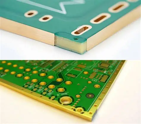
Copper weight refers to the thickness of the copper layer on a PCB, typically measured in ounces per square foot (oz/ft2). In practical terms, 1 oz/ft2 translates to a copper thickness of about 1.37 mils (0.00137 inches or 34.8 micrometers). Common copper weights for 4-layer PCBs range from 0.5 oz to 2 oz, with 1 oz being the standard for many applications. In a 4-layer PCB, copper weight can vary between layers—often, outer layers might have a different weight than inner layers depending on the design requirements.
The choice of copper weight in a 4-layer PCB directly affects several performance factors. Thicker copper (higher weight) can carry more current and improve heat dissipation, which is ideal for power distribution. However, it can also impact signal integrity, especially for high-speed signals, due to increased parasitic capacitance and manufacturing challenges. Understanding how copper weight influences a 4-layer PCB is the first step to optimizing your design.
4-Layer PCB Copper Weight and Current Carrying Capacity
One of the primary considerations when selecting copper weight for a 4-layer PCB is its current carrying capacity. This refers to the amount of electrical current a trace can safely handle without overheating or failing. The current carrying capacity depends on the cross-sectional area of the trace, which is determined by both the trace width and the copper thickness (weight).
For instance, a 1 oz copper trace with a width of 10 mils (0.01 inches) can typically handle around 1 ampere of current with a temperature rise of 10°C above ambient, based on industry standards like IPC-2221. If you increase the copper weight to 2 oz, the same 10-mil trace can handle roughly double the current—closer to 2 amperes—under the same conditions. This is because the thicker copper provides a larger cross-sectional area for current to flow through, reducing resistance and heat generation.
In a 4-layer PCB, current carrying capacity is especially important for power and ground planes, often placed on inner layers. Using a higher copper weight (like 2 oz) on these layers ensures that they can handle larger currents without voltage drops or excessive heat. However, thicker copper can increase manufacturing costs and board weight, so it’s a trade-off that needs careful evaluation based on your application.
4-Layer PCB Trace Width Calculation and Copper Weight
Calculating the appropriate trace width for a 4-layer PCB is a crucial step in ensuring that it can handle the required current while maintaining reliability. Trace width calculation depends on the copper weight, the expected current, and the allowable temperature rise. A common tool for this is a trace width calculator based on standards like IPC-2221, which provides guidelines for safe current limits.
Let’s break it down with an example. Suppose you’re designing a 4-layer PCB with a 1 oz copper layer, and a trace needs to carry 2 amperes of current with a temperature rise of no more than 10°C. Using a trace width calculator, you might find that a trace width of approximately 20 mils is required. If you switch to a 2 oz copper weight, the required trace width drops to around 10 mils for the same current and temperature rise, thanks to the increased thickness reducing resistance.
In a 4-layer PCB, trace width calculations are often more complex because of the layered structure. Power traces on inner layers may need wider widths or heavier copper to manage high currents, while signal traces on outer layers might prioritize thinner copper for better impedance control. Balancing these needs is key to a successful design, and online calculators or PCB design software can help simplify the process.
4-Layer PCB Signal Integrity and Copper Weight
Signal integrity is another critical factor in 4-layer PCB design, especially for high-speed applications like data communication or RF circuits. Signal integrity refers to the ability of a signal to travel through a trace without distortion, noise, or loss. Copper weight plays a significant role in this, as it affects the impedance of traces and the parasitic effects between layers.
In a 4-layer PCB, signal traces are often placed on the outer layers, with power and ground planes on the inner layers to provide shielding and reduce electromagnetic interference (EMI). A common stack-up might be Signal-Power-Ground-Signal. Using a lighter copper weight (e.g., 0.5 oz or 1 oz) on signal layers can help maintain controlled impedance, which is crucial for high-speed signals. For example, a 50-ohm impedance trace, common in RF designs, requires precise control of trace width and dielectric spacing, which can be easier to achieve with thinner copper.
However, if the copper weight is too light, it may lead to higher resistance, causing signal loss over long traces. Conversely, heavier copper (like 2 oz) can increase parasitic capacitance between layers, potentially causing crosstalk or signal delays in high-frequency designs. For a 4-layer PCB, signal integrity often requires a careful balance—using 1 oz copper on signal layers and heavier copper (1.5 oz or 2 oz) on power and ground planes is a common approach to optimize both signal quality and power delivery.
4-Layer PCB Power Distribution and Copper Weight
Effective power distribution is vital in a 4-layer PCB, especially for designs with multiple components requiring stable voltage and current. Copper weight significantly influences how well power is distributed across the board. Power and ground planes, often placed on the inner layers of a 4-layer PCB, benefit from heavier copper weights (1.5 oz or 2 oz) to minimize voltage drops and ensure even current distribution.
For example, in a design with a high-power microcontroller drawing 5 amperes, using a 1 oz copper plane might result in noticeable voltage drops across the board, leading to inconsistent performance. Switching to a 2 oz copper plane can reduce resistance, ensuring that the voltage remains stable even under high current loads. Additionally, heavier copper improves thermal management by dissipating heat more effectively, preventing hotspots that could damage components.
In terms of power distribution, 4-layer PCBs offer an advantage over 2-layer boards because dedicated power and ground planes reduce noise and improve decoupling. However, the copper weight must be chosen based on the total current requirements and the board’s thermal constraints. Over-specifying copper weight can increase costs unnecessarily, while under-specifying it risks performance issues. A well-designed 4-layer PCB will use copper weight strategically to balance cost and functionality for power distribution.
Balancing Trade-Offs: Copper Weight in 4-Layer PCB Design
Choosing the right copper weight for a 4-layer PCB involves balancing multiple factors: current carrying capacity, signal integrity, power distribution, thermal performance, and cost. Here are some key considerations to help guide your decision:
- Current Needs: For high-current applications, prioritize heavier copper (1.5 oz or 2 oz) on power and ground layers to handle the load without overheating.
- Signal Speed: For high-speed signals, lighter copper (0.5 oz or 1 oz) on signal layers can help maintain controlled impedance and reduce parasitic effects.
- Thermal Management: Heavier copper dissipates heat better, which is critical for power-intensive designs or compact boards with limited airflow.
- Cost and Manufacturability: Thicker copper increases material and manufacturing costs. It can also make etching finer traces more difficult, potentially limiting design flexibility.
In many cases, a hybrid approach works best. For instance, using 1 oz copper on outer signal layers and 2 oz on inner power and ground planes can provide a good balance for mixed-signal designs. Always simulate your design or consult with manufacturing guidelines to ensure that your chosen copper weights align with the board’s requirements and production capabilities.
Practical Tips for Selecting Copper Weight in 4-Layer PCBs
To wrap up, here are some actionable tips for selecting copper weight in your 4-layer PCB designs:
- Analyze Current Requirements: Calculate the maximum current for each layer and use trace width calculators to determine the necessary copper weight.
- Prioritize Stack-Up Design: Place power and ground planes on inner layers with heavier copper for stable power distribution, and use lighter copper on signal layers for better impedance control.
- Consider Signal Frequency: For high-frequency designs, test different copper weights to minimize signal loss and crosstalk.
- Account for Thermal Constraints: If your board operates in a high-temperature environment, opt for heavier copper to improve heat dissipation.
- Work Within Budget: Balance performance needs with cost by using heavier copper only where it’s necessary, such as on power planes.
By carefully considering these factors, you can optimize your 4-layer PCB for both performance and reliability. Copper weight is not a one-size-fits-all decision—it’s a design parameter that must be tailored to your specific application.
Conclusion: Mastering Copper Weight in 4-Layer PCB Design
Copper weight is a foundational element in the design of 4-layer PCBs, influencing everything from current carrying capacity to signal integrity and power distribution. By understanding how different copper weights impact these aspects, you can make informed choices that enhance the performance and longevity of your circuit boards. Whether you’re calculating trace widths for a high-current power plane or fine-tuning signal layers for high-speed data, copper weight is a variable you can’t overlook.
At ALLPCB, we’re committed to helping you navigate the complexities of PCB design. With the right balance of copper weight and thoughtful layer planning, your 4-layer PCB can achieve optimal performance for any application. Use the insights and tips shared in this guide to refine your designs, and ensure that every layer of your board works in harmony to deliver reliable results.
 ALLPCB


