 ALLPCB


Designing a compact ECU PCB (Electronic Control Unit Printed Circuit Board) for limited space environments is a critical skill in modern automotive design. With vehicles becoming smarter and more compact, engineers face the challenge of fitting powerful electronics into tight spaces without compromising performance or reliability. This guide will walk you through the essential steps and techniques for creating a compact ECU PCB, focusing on PCB miniaturization, automotive PCB design, PCB component placement, and High Density Interconnect (HDI) technology. Whether you're working on electric vehicles or advanced driver-assistance systems (ADAS), these strategies will help you optimize space while meeting strict automotive standards.
Let’s dive into the details of designing a space-efficient ECU PCB that delivers high performance in constrained environments.
Why Compact ECU PCB Design Matters in Automotive Applications
In the automotive industry, space is often at a premium. Modern vehicles are packed with electronic systems for engine control, safety features, and infotainment, all of which rely on ECUs. These control units must fit into small compartments, often near heat sources or in areas prone to vibration. A compact ECU PCB not only saves space but also reduces weight, improves thermal management, and lowers production costs.
Moreover, automotive PCB design must adhere to stringent standards for durability and signal integrity. A poorly designed PCB can lead to electromagnetic interference (EMI), signal delays, or component failure under harsh conditions. By focusing on PCB miniaturization and efficient PCB component placement, you can ensure reliability while meeting space constraints.
Key Challenges in Designing Compact ECU PCBs
Before we explore the solutions, it’s important to understand the challenges of designing for limited space environments:
- Space Constraints: ECUs often need to fit into tight spaces, leaving little room for large boards or bulky components.
- Thermal Management: Smaller boards can lead to heat buildup, especially in high-power automotive applications.
- Signal Integrity: Close component placement can cause crosstalk or EMI, affecting performance.
- Manufacturing Limits: Miniaturized designs often require advanced fabrication techniques, which can increase costs if not planned properly.
With these challenges in mind, let’s look at proven strategies to design a compact ECU PCB.
Step 1: Leverage High Density Interconnect (HDI) Technology
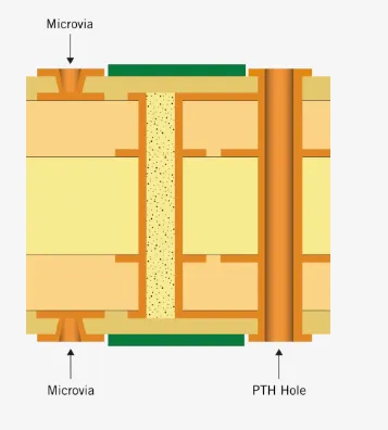
One of the most effective ways to achieve PCB miniaturization is by using High Density Interconnect (HDI) technology. HDI PCBs allow for finer traces, smaller vias, and higher component density compared to traditional boards. This technology is ideal for automotive applications where space is limited but performance cannot be compromised.
HDI boards use microvias (vias with diameters less than 0.15 mm) and buried vias to connect layers, reducing the board’s overall footprint. For example, in an ECU controlling an electric vehicle’s battery management system, HDI can help pack complex circuitry into a board as small as 50 mm x 50 mm while maintaining signal integrity at frequencies up to 1 GHz.
Benefits of HDI for Compact ECU PCB Design:
- Reduces board size by up to 30% compared to standard PCBs.
- Allows for more components per square inch, critical for multifunctional ECUs.
- Improves signal performance by minimizing trace lengths and reducing impedance mismatches (typical impedance control at 50 ohms for high-speed signals).
Step 2: Optimize PCB Component Placement for Space Efficiency
Effective PCB component placement is the foundation of a compact design. Poor placement can lead to wasted space, longer traces, and increased risk of interference. Here are actionable tips to maximize space utilization on your ECU PCB:
Group Components by Function: Place components with related functions close together to minimize trace lengths. For instance, group power management ICs near capacitors and inductors to reduce noise in power delivery networks.
Use Both Sides of the Board: In tight spaces, utilize both the top and bottom layers of the PCB for component placement. Surface-mount devices (SMDs) with low profiles (e.g., 0402 or 0201 package sizes) are ideal for this approach.
Prioritize High-Power Components: Place heat-generating components like voltage regulators or power transistors near the edges of the board or close to heat sinks. This prevents thermal buildup in the center of the compact ECU PCB, where cooling is harder.
Minimize Connector Size: Use miniaturized connectors and avoid bulky through-hole components. For example, switching to a 0.5 mm pitch connector instead of a 1.0 mm pitch can save significant space.
By carefully planning component placement, you can reduce the board size by up to 20% while maintaining functionality and reliability.
Step 3: Implement Multi-Layer Designs for PCB Miniaturization
In limited space environments, a single-layer or double-layer PCB often isn’t enough to handle the complexity of an ECU. Multi-layer designs, combined with HDI technology, allow you to stack circuits vertically, significantly reducing the board’s footprint.
For instance, a 6-layer PCB with a thickness of 1.6 mm can accommodate high-speed signals, power planes, and ground planes while keeping the board size under 60 mm x 40 mm. Separate layers for power and ground also help reduce EMI, a common issue in automotive PCB design.
Key Tips for Multi-Layer Design:
- Use dedicated layers for high-speed signals to maintain signal integrity (e.g., keep differential pairs on inner layers with controlled impedance of 100 ohms).
- Place ground planes adjacent to signal layers to minimize noise.
- Optimize via placement to avoid overcrowding; use blind and buried vias to save space.
Multi-layer designs are especially useful for ECUs managing multiple systems, such as engine control and sensor data processing, in a single compact unit.
Step 4: Focus on Thermal Management in Compact Designs
A smaller ECU PCB means components are closer together, increasing the risk of overheating. In automotive environments, where temperatures can range from -40°C to 85°C, thermal management is non-negotiable.
Strategies for Effective Cooling:
- Thermal Vias: Place thermal vias under high-power components to transfer heat to a ground plane or heat sink. For example, a grid of 0.3 mm vias under a power IC can reduce junction temperature by 10-15°C.
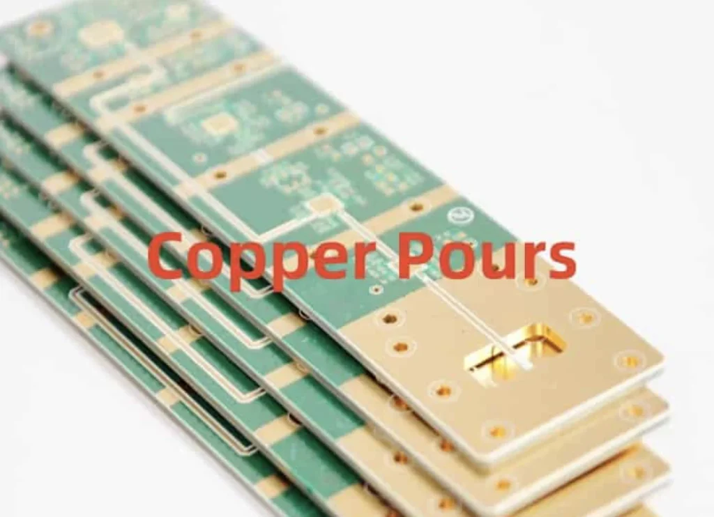
- Copper Pours: Use large copper areas connected to ground or power planes to dissipate heat across the board.
- Component Spacing: Even in compact designs, maintain a minimum spacing (e.g., 0.5 mm) around hot components to prevent heat concentration.
Proper thermal design ensures your ECU PCB operates reliably under harsh conditions, extending its lifespan in automotive applications.
Step 5: Ensure Signal Integrity in High-Density Designs
In a compact ECU PCB, maintaining signal integrity is challenging due to shorter distances between traces and components. High-speed signals, such as those used in CAN bus or Ethernet communication in vehicles, are particularly vulnerable to crosstalk and impedance issues.
Best Practices for Signal Integrity:
- Controlled Impedance: Design traces with specific widths and spacing to achieve target impedance (e.g., 50 ohms for single-ended signals or 100 ohms for differential pairs).
- Short Trace Lengths: Keep high-speed signal traces as short as possible to reduce signal delay and loss. For instance, a trace length under 50 mm can keep delays below 300 ps for signals at 1 GHz.
- Ground Planes: Use continuous ground planes under signal layers to provide a return path and minimize EMI.
By prioritizing signal integrity, your ECU PCB can handle high-speed data without errors, even in a miniaturized layout.
Step 6: Test and Validate Your Compact ECU PCB Design
Once your design is complete, thorough testing is essential to ensure it meets automotive standards. Compact designs are more prone to issues like thermal stress or signal interference, so validation is a critical step.
Testing Methods:
- Simulation Tools: Use simulation software to analyze signal integrity, thermal performance, and EMI before manufacturing. For example, simulate power delivery networks to ensure voltage drops are below 5%.
- Prototyping: Build a prototype to test real-world performance under temperature and vibration stress (e.g., MIL-STD-810G standards for automotive environments).
- Compliance Checks: Verify that your design meets automotive standards like ISO 26262 for functional safety and AEC-Q100 for component reliability.
Testing helps identify and fix issues early, saving time and cost in the long run.
Conclusion: Mastering Compact ECU PCB Design
Designing a compact ECU PCB for limited space environments requires a combination of advanced techniques like High Density Interconnect (HDI), strategic PCB component placement, and careful attention to thermal and signal integrity concerns. By leveraging PCB miniaturization strategies and adhering to automotive PCB design best practices, you can create reliable, high-performance ECUs that fit into the tightest spaces without sacrificing functionality.
Start with HDI technology to shrink your board size, optimize component placement for efficiency, and use multi-layer designs to pack more functionality into less space. Don’t forget to address thermal management and signal integrity to ensure your ECU performs flawlessly under harsh automotive conditions. Finally, validate your design through simulation and testing to guarantee reliability.
With these steps, you’ll be well-equipped to tackle the challenges of designing compact ECU PCBs, delivering innovative solutions for modern vehicles. If you’re ready to bring your design to life, explore advanced PCB fabrication options to support your miniaturized, high-density layouts.


