 ALLPCB


In the world of aerospace technology, precision and reliability are non-negotiable. If you're looking for insights on 8-layer PCB aerospace standards or how to design an 8-layer PCB high-reliability design for extreme conditions, you've come to the right place. This blog dives deep into the critical aspects of designing 8-layer printed circuit boards (PCBs) for aerospace applications, focusing on meeting stringent requirements like vibration resistance, thermal stability, and radiation protection. We'll explore the design considerations, testing protocols, and hardening techniques to ensure your PCBs perform flawlessly in the harshest environments.
At ALLPCB, we understand the unique challenges of aerospace electronics. Whether you're an engineer working on satellite systems or avionics, this guide will provide actionable insights to help you design robust 8-layer PCBs that meet industry standards. Let's break down the key elements step by step.
Why Choose an 8-Layer PCB for Aerospace Applications?
Aerospace systems demand complex electronics with high performance and compact designs. An 8 layer PCB offers the perfect balance between functionality and space efficiency. With eight conductive layers, these boards allow for intricate routing, better signal integrity, and enhanced power distribution—crucial for avionics, satellite communication, and defense systems.
Unlike simpler 2- or 4 layer PCBs, an 8-layer PCB can handle high-speed signals with minimal interference, thanks to dedicated ground and power planes. This is vital in aerospace, where a single signal error can lead to catastrophic failure. Additionally, the multilayer structure supports advanced shielding against electromagnetic interference (EMI), a common concern in high-altitude or space environments.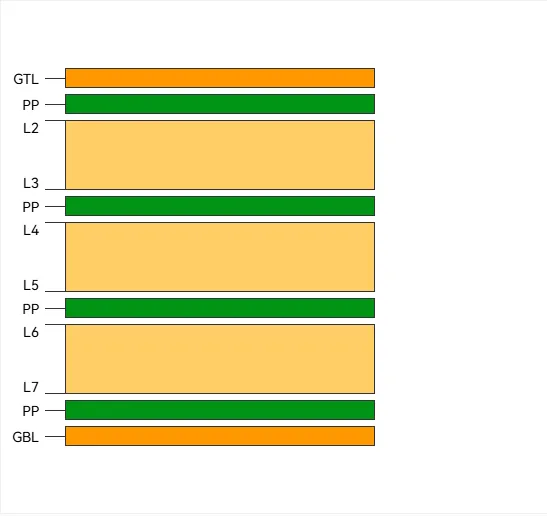
Key Challenges in Aerospace PCB Design
Designing an 8-layer PCB for aerospace isn't just about stacking layers. It involves addressing extreme conditions that standard PCBs can't withstand. Here are the primary challenges engineers face:
- Extreme Temperatures: Aerospace PCBs must operate in temperatures ranging from -55°C to 125°C or higher, especially in space or high-altitude environments.
- Vibration and Mechanical Stress: Launch conditions and in-flight turbulence subject PCBs to intense vibrations and shocks.
- Radiation Exposure: In space, cosmic rays and solar radiation can degrade electronic components over time.
- Signal Integrity: High-speed data transmission in aerospace systems requires impeccable signal quality, often at frequencies exceeding 1 GHz.
- Size and Weight Constraints: Every gram matters in aerospace, so PCBs must be compact yet powerful.
Meeting these challenges requires adherence to strict 8-layer PCB aerospace standards and innovative design strategies. Let's explore how to address each of these issues in detail.
Adhering to 8-Layer PCB Aerospace Standards
Aerospace PCBs must comply with rigorous industry standards to ensure safety and reliability. Standards like IPC-6012 (Qualification and Performance Specification for Rigid Printed Boards) and MIL-PRF-31032 (Military Specification for Printed Circuit Boards) set the benchmark for design and manufacturing. For space applications, additional guidelines from organizations like NASA and the European Space Agency (ESA) often apply.
These standards dictate everything from material selection to trace width and spacing. For instance, dielectric thickness in an 8-layer PCB should be at least 3.5 mils to provide sufficient mechanical strength under stress. Copper thickness for power planes might range from 1 to 2 ounces per square foot to handle high current loads without overheating. Ensuring compliance with these standards during the design phase is critical to passing qualification tests later.
At ALLPCB, we prioritize manufacturing processes that align with these strict guidelines, ensuring that every 8-layer PCB meets the necessary certifications for aerospace use.
Designing for High Reliability: 8-Layer PCB High-Reliability Design
Reliability is the cornerstone of aerospace electronics. An 8-layer PCB high-reliability design starts with selecting the right materials and layout strategies to minimize failure risks. Here are key considerations:
Material Selection
Standard FR-4 materials often fall short in aerospace due to poor thermal and mechanical properties. Instead, high-performance materials like polyimide or PTFE-based laminates are preferred. These materials offer a higher glass transition temperature (Tg) of over 180°C, ensuring stability under thermal stress. They also provide better resistance to outgassing—a critical factor in vacuum environments like space.
Suggested Reading: 8-Layer PCB Stackup: Choosing the Right Materials for Your Application
Layer Stack-Up Optimization
The arrangement of layers in an 8-layer PCB directly impacts performance. A typical stack-up might include alternating signal and ground planes to reduce crosstalk and EMI. For example:
- Layer 1: Signal (Top)
- Layer 2: Ground
- Layer 3: Signal
- Layer 4: Power
- Layer 5: Power
- Layer 6: Signal
- Layer 7: Ground
- Layer 8: Signal (Bottom)
This configuration ensures controlled impedance, often targeting values like 50 ohms for high-speed signals, and minimizes noise interference.
Component Placement and Routing
Components must be placed to avoid thermal hotspots and mechanical stress points. Critical components should be near ground planes for better heat dissipation. Routing should prioritize short, direct traces to reduce signal delay, with differential pairs maintained at a consistent spacing (e.g., 5 mils) to prevent skew.
By focusing on these design principles, an 8-layer PCB can achieve the high reliability needed for mission-critical aerospace systems.
Ensuring Durability with 8-Layer PCB Vibration Testing
Vibration is a major concern during rocket launches and high-speed flights. 8-layer PCB vibration testing simulates these conditions to ensure the board can withstand mechanical stress without cracking or losing connectivity. Testing often follows standards like MIL-STD-810, which defines vibration profiles for aerospace equipment.
During testing, PCBs are subjected to random vibrations across a frequency range of 20 Hz to 2000 Hz, with acceleration levels up to 20 g. Solder joints, vias, and component attachments are closely inspected for failures. To pass these tests, designers must use reinforced mounting holes and secure components with adhesives or conformal coatings to dampen vibrations.
Additionally, finite element analysis (FEA) during the design phase can predict stress points on the PCB. By identifying weak areas, engineers can reinforce the board with thicker copper or additional vias before manufacturing.
Managing Extreme Temperatures with 8-Layer PCB Thermal Cycling
Temperature fluctuations in aerospace environments can cause expansion and contraction, leading to cracks or delamination in PCBs. 8-layer PCB thermal cycling tests evaluate a board's ability to endure these changes, typically cycling between -55°C and 125°C for hundreds of cycles as per IPC-TM-650 standards.
To survive thermal cycling, an 8-layer PCB must use materials with a low coefficient of thermal expansion (CTE), ideally below 15 ppm/°C, to match the CTE of components and prevent stress. Thermal vias can also be added near high-power components to transfer heat away from sensitive areas, maintaining a temperature gradient below 10°C across the board.
Proper thermal management in the design phase, combined with rigorous testing, ensures that the PCB remains operational through extreme temperature shifts encountered in flight or space missions.
Protecting Against Radiation with 8-Layer PCB Radiation Hardening
In space, radiation poses a significant threat to electronics, causing bit flips, latch-ups, or complete failure. 8-layer PCB radiation hardening is essential for protecting circuits from cosmic rays and solar particles. Hardening techniques include:
- Shielding: Adding protective layers or enclosures around the PCB to block radiation. While this increases weight, strategic placement can minimize the impact.
- Radiation-Tolerant Components: Using components rated for total ionizing dose (TID) levels of 100 krad or higher ensures longevity in space.
- Error Correction: Implementing error-correcting code (ECC) memory and redundant systems in the design to mitigate radiation-induced errors.
Ground testing for radiation hardness often involves exposing the PCB to gamma rays or heavy ions to simulate space conditions. Designers can use simulation tools to predict single-event effects (SEE) and adjust layouts to minimize vulnerable areas, such as spacing critical traces further apart.
By incorporating these hardening methods, an 8-layer PCB can maintain functionality even in high-radiation environments, ensuring mission success.
Manufacturing and Quality Assurance for Aerospace PCBs
Even the best design is useless without precise manufacturing and thorough quality checks. For 8-layer PCBs in aerospace, every step—from lamination to soldering—must meet exact tolerances. Automated optical inspection (AOI) and X-ray testing verify layer alignment and via integrity, ensuring no hidden defects.
Conclusion: Building the Future of Aerospace with 8-Layer PCBs
Designing an 8-layer PCB for aerospace applications is a complex but rewarding endeavor. By focusing on 8-layer PCB aerospace standards, prioritizing 8-layer PCB high-reliability design, and rigorously testing for vibration, thermal, and radiation challenges, engineers can create electronics that withstand the harshest environments. Whether it's through 8-layer PCB vibration testing, 8-layer PCB thermal cycling, or 8-layer PCB radiation hardening, every detail matters in ensuring mission success.
At ALLPCB, we're committed to supporting aerospace innovation with high-quality PCB solutions. Our expertise in multilayer designs and adherence to industry standards make us a trusted partner for your next project. Ready to take your aerospace electronics to new heights? Start with a robust 8-layer PCB design tailored to meet stringent requirements.


