 ALLPCB


In the world of advanced electronics, 16-layer PCBs are a cornerstone for high-performance and compact designs. A critical aspect of these multilayer boards is via technology, which ensures reliable interlayer connections in dense layouts. If you're wondering how to optimize via design for a 16-layer PCB, the answer lies in understanding and leveraging various via types like microvias, blind vias, buried vias, and via-in-pad solutions, especially in High-Density Interconnect (HDI) technology. This blog dives deep into the specifics of via technology, offering practical insights to enhance your PCB designs for efficiency and performance.
Why Via Technology Matters in 16-Layer PCB Design
Modern electronics demand more functionality in smaller spaces, pushing the boundaries of PCB design. A 16-layer PCB, with its multiple layers of conductive traces and insulating materials, is ideal for complex applications like telecommunications, medical devices, and aerospace systems. However, connecting these layers effectively requires advanced via technology. Vias are small conductive pathways that link different layers of a PCB, enabling electrical signals and power to flow seamlessly.
In dense designs, improper via placement or type selection can lead to signal integrity issues, increased impedance, or even manufacturing challenges. For instance, a poorly designed via might introduce a delay in signal transmission, impacting performance in high-speed circuits operating at frequencies above 1 GHz. By optimizing via technology, you can minimize these risks, reduce board space, and improve overall reliability.
Understanding the Basics of Vias in 16-Layer PCBs
Before diving into specific via types, let’s cover the fundamental role of vias in a 16-layer PCB. Vias are essentially plated holes that create electrical connections between layers. In a board with 16 layers, vias can span all layers or connect only specific ones, depending on the design needs. Their size, placement, and type directly impact the board’s performance, manufacturability, and cost.
In high-density designs, traditional through-hole vias—drilled from the top to the bottom of the board—often waste valuable space. This is where advanced via technologies come into play, allowing for more compact and efficient layouts. Let’s explore the key via types used in 16-layer PCB via design and their unique benefits.
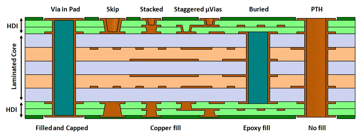
1. Microvias: Precision for HDI PCB Technology
Microvias are small-diameter vias, typically less than 0.15 mm (6 mils), created using laser drilling. They are a hallmark of HDI PCB technology, which is often employed in 16-layer boards to achieve higher component density. Microvias connect only adjacent layers or a few layers, reducing the space needed compared to traditional vias.
For example, in a smartphone motherboard, microvias allow designers to place more components in a limited area while maintaining signal integrity at high frequencies (up to 5 GHz or more). They also lower parasitic capacitance and inductance, which can otherwise degrade performance in high-speed designs. However, microvias require precise manufacturing processes, and their aspect ratio (depth-to-diameter) must be carefully controlled—ideally below 1:1—to ensure reliability.
2. Blind Vias: Surface-to-Inner Layer Connections
Blind vias connect an outer layer of the PCB to one or more inner layers without passing through the entire board. In a 16-layer PCB, blind vias are useful for freeing up space on the opposite side of the board, allowing for additional routing or component placement. They are often used in designs where surface space is at a premium, such as in compact consumer electronics.
Blind vias, with diameters as small as 0.1 mm in advanced designs, help reduce signal stub lengths, which can cause reflections in high-speed signals traveling at speeds exceeding 2.5 Gbps. By minimizing these stubs, blind vias improve signal integrity. However, their manufacturing involves sequential lamination, which can increase production costs compared to standard through-hole vias.
3. Buried Vias: Hidden Connections for Inner Layers
Buried vias are located entirely within the inner layers of a PCB, invisible from the outer surfaces. In a 16-layer PCB, buried vias connect internal layers without affecting the outer layers, maximizing space for surface-mounted components. They are particularly valuable in dense designs where every square millimeter counts.
For instance, in a multilayer server board, buried vias can route signals between layers 4 and 6 without interfering with the top or bottom layers. This reduces the need for additional signal layers, potentially lowering the overall layer count and cost. Like blind vias, buried vias require advanced fabrication techniques, such as multiple lamination cycles, which must be accounted for during the design phase.
4. Via-in-Pad: Maximizing Space in Dense Layouts
Via-in-pad technology involves placing a via directly within the pad of a surface-mounted component, such as a BGA (Ball Grid Array) package. In 16-layer PCB via design, this approach is a game-changer for ultra-dense layouts where traditional via placement would consume too much space. By integrating the via into the pad, you eliminate the need for additional routing space, allowing for tighter component placement.
Via-in-pad is commonly used in HDI PCB designs for applications like high-end processors or memory modules, where pin counts can exceed 1000. However, this method requires careful consideration of thermal management, as solder can flow into the via during assembly, potentially causing voids. To mitigate this, vias are often filled with conductive or non-conductive materials and capped with a planar surface. This ensures a stable connection while maintaining a compact footprint.
The Role of HDI PCB Technology in 16-Layer Designs
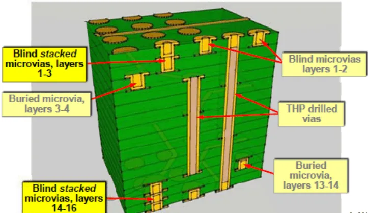
High-Density Interconnect (HDI) technology is synonymous with advanced 16-layer PCB designs. HDI PCBs use a combination of microvias, blind vias, and buried vias to achieve finer trace widths (as low as 0.075 mm or 3 mils) and tighter spacing. This allows for more connections in a smaller area, making HDI ideal for cutting-edge devices like wearables, IoT modules, and 5G equipment.
In HDI designs, microvias are often stacked or staggered to connect multiple layers efficiently. For example, a stacked microvia configuration might connect layers 1 to 2 and 2 to 3, forming a continuous path without occupying extra space. This reduces the board’s overall thickness and enhances signal performance by shortening connection lengths. However, designers must balance the benefits of HDI with manufacturing constraints, as stacking more than two or three microvias can increase the risk of defects.
Best Practices for Optimizing Via Design in 16-Layer PCBs
Designing vias for a 16-layer PCB requires a strategic approach to balance performance, cost, and manufacturability. Here are some actionable tips to optimize interlayer connections in dense designs:
- Choose the Right Via Type: Use microvias and blind vias for surface-to-inner connections in HDI layouts, and reserve buried vias for internal routing to save space. Avoid overusing through-hole vias unless necessary for power distribution or thermal management.
- Minimize Via Size: Opt for smaller via diameters (e.g., 0.1–0.2 mm for microvias) to reduce parasitic effects and save board space. Ensure the aspect ratio remains within manufacturer-recommended limits, typically 0.75:1 for microvias, to avoid drilling issues.
- Plan for Signal Integrity: Place vias strategically to avoid long stubs that can cause signal reflections, especially in high-speed designs operating above 1 GHz. Use simulation tools to analyze impedance, targeting values like 50 ohms for controlled impedance lines.
- Consider Thermal Management: For via-in-pad designs, ensure proper filling and capping to prevent solder wicking during assembly. Add thermal vias if heat dissipation is a concern, spacing them evenly under high-power components.
- Collaborate with Manufacturers: Work closely with your PCB fabrication partner to align via designs with their capabilities. Confirm minimum drill sizes, lamination cycles, and via filling options to avoid costly redesigns.
Challenges and Solutions in 16-Layer PCB Via Design
While advanced via technologies offer numerous benefits, they also come with challenges. One common issue is the increased complexity of manufacturing. For instance, laser-drilled microvias in HDI PCBs require precise alignment, and any deviation can lead to open circuits or reliability failures. To address this, designers should adhere to strict design rules, such as maintaining a minimum annular ring of 0.05 mm around vias for stability.
Another challenge is cost. The use of blind and buried vias, along with multiple lamination steps, can drive up production expenses by 20–30% compared to standard multilayer boards. A practical solution is to optimize the layer stack-up early in the design process, using only the necessary number of advanced vias to meet performance goals.
Finally, signal integrity remains a critical concern in dense 16-layer designs. Vias can introduce crosstalk or impedance mismatches if not designed properly. To mitigate this, maintain consistent trace widths (e.g., 0.1 mm for high-speed signals) and use ground planes near vias to shield against interference.
Future Trends in Via Technology for Multilayer PCBs
As electronics continue to evolve, via technology is keeping pace with new innovations. One emerging trend is the use of advanced materials for via filling, such as conductive pastes that improve thermal conductivity by up to 10 W/m·K, enhancing heat dissipation in high-power applications. Another development is the adoption of optical vias for ultra-high-speed data transmission, potentially supporting rates beyond 100 Gbps in future 16-layer designs.
Additionally, automation in PCB design software is making via optimization more accessible. Tools now offer real-time analysis of via placement, predicting signal delays and impedance issues before fabrication. These advancements promise to simplify the design process while pushing the limits of density and performance in multilayer boards.
Conclusion: Mastering Via Technology for 16-Layer PCB Success
Via technology is at the heart of effective 16-layer PCB design, enabling reliable interlayer connections in even the most dense and complex layouts. By leveraging microvias, blind vias, buried vias, and via-in-pad solutions within the framework of HDI PCB technology, designers can achieve compact, high-performance boards for cutting-edge applications. The key is to balance design innovation with manufacturing realities, ensuring that every via serves a purpose without compromising reliability or cost.
Whether you’re working on telecommunications equipment, medical devices, or consumer electronics, understanding and optimizing via design will elevate your 16-layer PCB projects. With careful planning and adherence to best practices, you can tackle the challenges of dense designs and deliver solutions that meet the demands of today’s technology landscape.


