ALLPCB


In the world of printed circuit board (PCB) design and assembly, clarity is everything. One often overlooked factor that plays a crucial role in ensuring precision and reducing errors is PCB silkscreen resolution. But why is PCB silkscreen resolution important, and how does it impact component identification on a PCB? Simply put, silkscreen resolution determines how clearly markings like component labels, test points, and symbols appear on the board. High-resolution silkscreen ensures better legibility, which helps engineers and assemblers identify components accurately, ultimately minimizing PCB assembly errors.
In this comprehensive guide, we’ll dive deep into the significance of silkscreen resolution, explore its role in component identification, discuss silkscreen legibility standards, and highlight how it can prevent costly mistakes during assembly. Whether you’re a PCB designer, engineer, or manufacturer, understanding these concepts can elevate the quality of your projects. Let’s unlock the secrets of PCB clarity together.
What Is PCB Silkscreen and Why Does It Matter?
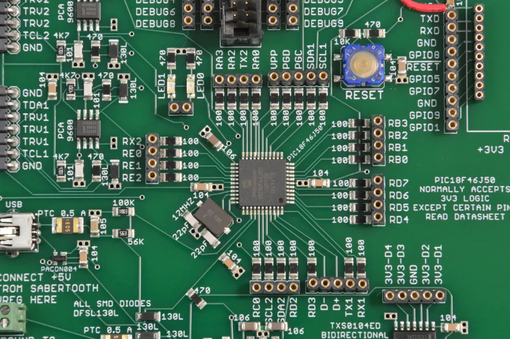
PCB silkscreen, often referred to as the legend layer, is a non-conductive ink layer applied to the surface of a printed circuit board. This layer includes text, symbols, and markings that provide critical information about the board’s components, test points, and assembly instructions. Typically, silkscreen is printed in white, yellow, or black ink on the component or solder side of the PCB, depending on the design requirements.
The primary purpose of silkscreen is to act as a visual guide. It helps engineers, technicians, and assemblers quickly identify components like resistors, capacitors, and ICs by displaying reference designators (e.g., R1 for a resistor, C3 for a capacitor). Additionally, it may include polarity indicators, pin numbers, or warning symbols to ensure correct assembly and troubleshooting.
However, the effectiveness of silkscreen depends heavily on its resolution. Low-resolution silkscreen can result in blurred or unreadable text, leading to confusion during assembly or testing. On the other hand, high-resolution silkscreen offers sharp, clear markings that streamline the process and reduce errors. This is where the importance of PCB silkscreen resolution comes into play, directly impacting component identification and overall project success.
The Importance of PCB Silkscreen Resolution
PCB silkscreen resolution refers to the sharpness and detail of the printed markings on the board. It is typically measured in dots per inch (DPI), with higher DPI values indicating better clarity. For instance, a silkscreen printed at 600 DPI will appear much clearer than one at 300 DPI, especially for small text or intricate symbols.
High-resolution silkscreen is critical for several reasons:
- Improved Legibility: Clear markings ensure that even tiny text (as small as 4-point font) remains readable under magnification or normal viewing conditions. This is essential for dense PCB layouts with numerous components.
- Accurate Component Identification: Misreading a component label like “R10” as “R18” due to poor resolution can lead to incorrect part placement, causing functional failures.
- Reduced Assembly Errors: During manual or automated assembly, technicians rely on silkscreen markings to place components correctly. High-resolution printing minimizes the risk of misinterpretation.
- Faster Troubleshooting: During testing or repairs, engineers use silkscreen labels to locate specific components or test points. Clear markings speed up this process significantly.
Consider a scenario where a PCB design includes hundreds of components packed into a small area. If the silkscreen resolution is low, labels may overlap or become smudged, making it nearly impossible to distinguish between components without referring to design files. This not only slows down the assembly process but also increases the likelihood of costly mistakes.
How Silkscreen Resolution Impacts Component Identification on PCBs
Component identification on a PCB is the process of recognizing and locating specific parts based on silkscreen markings. These markings typically include reference designators, polarity indicators, and sometimes part numbers or values (e.g., “10k” for a 10-kiloohm resistor). When silkscreen resolution is high, these identifiers are crisp and easy to read, ensuring accurate placement and soldering.
Let’s break down how resolution directly affects component identification:
- Small Text and Symbols: Modern PCBs often feature miniature components with labels in tiny fonts. A resolution of at least 600 DPI is often necessary to render text smaller than 6-point size without distortion.
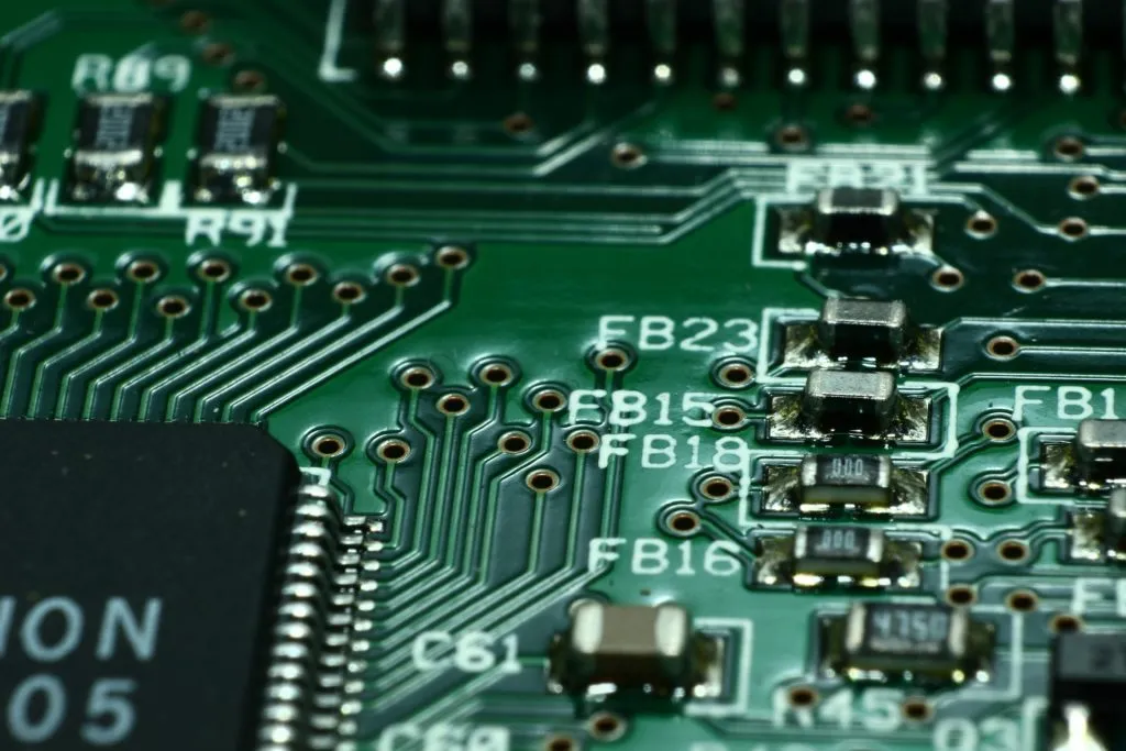
- Dense Layouts: In high-density designs, components are placed close together, leaving little room for silkscreen labels. High resolution prevents text from bleeding into adjacent markings, maintaining clarity.
- Polarity and Orientation: Components like diodes, capacitors, and ICs require correct orientation. High-resolution silkscreen ensures that polarity symbols (e.g., “+” for positive) or pin 1 indicators are visible and unambiguous.
For example, imagine assembling a board with a surface-mount IC that has 48 pins in a 7mm x 7mm package. The silkscreen must clearly mark pin 1 to ensure proper alignment. If the resolution is too low, the dot or triangle indicating pin 1 might be indistinguishable, leading to a misaligned chip and a non-functional board.
PCB Assembly Errors: The Cost of Poor Silkscreen Resolution
PCB assembly errors can be catastrophic, leading to delays, increased costs, and even product failures. While there are many causes of assembly mistakes, poor silkscreen resolution is a significant contributor that is often underestimated. Here’s how low-resolution silkscreen can lead to errors during assembly:
- Misplaced Components: If a label is unreadable, an assembler might place a component in the wrong spot. For instance, swapping a 1uF capacitor with a 10uF one due to unclear text can alter circuit behavior.
- Incorrect Orientation: Components like LEDs or transistors must be oriented correctly. Blurry polarity markers can result in reversed placement, damaging the component or circuit during power-up.
- Delayed Production: Assemblers may need to cross-reference unclear markings with design files, slowing down the process and increasing labor costs.
- Failed Quality Checks: Boards with assembly errors often fail testing, requiring rework or scrapping, which impacts timelines and budgets.
Studies in electronics manufacturing suggest that human error during manual assembly accounts for up to 30% of PCB defects. While automation reduces this risk, even pick-and-place machines rely on silkscreen for initial setup and verification. Investing in high-resolution silkscreen printing can save thousands of dollars by preventing these issues upfront.
Silkscreen Legibility Standards: What You Need to Know
To ensure consistent quality, the electronics industry follows silkscreen legibility standards set by organizations like the Institute of Printed Circuits (IPC). These guidelines help designers and manufacturers achieve readable and functional silkscreen layers. Some key standards related to silkscreen legibility include:
- Minimum Text Height: IPC-A-610, a widely accepted standard for PCB assembly, recommends a minimum text height of 0.040 inches (1mm) for silkscreen markings to ensure readability. However, for densely packed boards, smaller text may be used if printed at high resolution (600 DPI or higher).
- Line Width: The minimum line width for silkscreen strokes should be 0.006 inches (0.15mm) to prevent blurring or fading during printing.
- Contrast: Silkscreen ink color must contrast with the PCB surface. For example, white ink is often used on green or black solder masks for better visibility.
- Placement: Markings should not overlap with pads, vias, or other components to avoid confusion. IPC standards suggest a clearance of at least 0.010 inches (0.25mm) from copper features.
Adhering to these standards ensures that silkscreen remains legible under various lighting conditions and during different stages of manufacturing. Many PCB design tools also include built-in checks to verify compliance with these guidelines before fabrication begins.
Best Practices for Optimizing Silkscreen Resolution in PCB Design
Achieving high silkscreen resolution starts with thoughtful design and collaboration with your manufacturing partner. Here are some actionable tips to ensure clarity and precision in your PCB silkscreen:
- Use Vector-Based Graphics: Design silkscreen layers using vector formats rather than raster images. Vectors maintain sharpness regardless of scaling, ensuring high-resolution output.
- Choose Appropriate Fonts: Stick to simple, sans-serif fonts like Arial or Helvetica for better readability. Avoid overly stylized fonts that may distort at small sizes.
- Specify Resolution Requirements: Communicate with your manufacturer about the desired DPI for silkscreen printing. Most modern facilities can achieve 600-1200 DPI for crisp results.
- Prioritize Critical Markings: If space is limited, focus on essential labels like reference designators and polarity indicators. Avoid cluttering the board with unnecessary text.
- Test Print Samples: Before full production, request a sample board to verify silkscreen clarity under real-world conditions. Use a magnifying glass if needed to check small text.
By following these practices, you can significantly improve component identification and reduce the risk of errors during assembly. A well-designed silkscreen layer not only aids in manufacturing but also enhances the professional appearance of your PCB.
The Future of PCB Silkscreen Technology
As PCB designs become more complex with shrinking component sizes and higher densities, the demand for advanced silkscreen technology continues to grow. Innovations like laser-direct imaging (LDI) for silkscreen printing are emerging, offering resolutions as high as 2400 DPI for ultra-fine markings. Additionally, digital printing methods are being explored to allow customizable silkscreen layers without the need for traditional stencils, reducing setup time and costs.
Another trend is the integration of augmented reality (AR) in PCB assembly. While silkscreen remains essential, AR tools can overlay digital labels on physical boards, supplementing physical markings with interactive data. However, until such technologies become mainstream, high-resolution silkscreen will remain the backbone of component identification and error prevention.
Conclusion: Elevate Your PCB Projects with High-Resolution Silkscreen
In the intricate world of PCB design and assembly, every detail matters. The impact of silkscreen resolution on component identification cannot be overstated—it directly influences the accuracy, efficiency, and reliability of your projects. By prioritizing high-resolution silkscreen, adhering to legibility standards, and following best practices, you can minimize PCB assembly errors and ensure a smoother manufacturing process.
Whether you’re designing a simple prototype or a complex multilayer board, remember that clarity starts with a well-executed silkscreen layer. Invest in quality printing, collaborate closely with your manufacturing partner, and watch as your PCBs achieve new levels of precision and professionalism. Unlocking PCB clarity is not just about aesthetics; it’s about building better, more reliable electronics for the future.