 ALLPCB


In the fast-evolving world of electronics, the demand for smaller, faster, and more efficient printed circuit boards (PCBs) is at an all-time high. So, how do manufacturers achieve this level of miniaturization and performance? The answer lies in laser drilling—a cutting-edge technology that enables the creation of tiny, precise holes and vias for high-density interconnects. In this blog, we’ll explore the power of laser drilling for high-speed PCBs, its advantages, and how it drives PCB miniaturization and via formation for modern electronics.
Whether you're an engineer designing compact devices or a manufacturer looking to optimize production, understanding laser drilling can transform your approach to PCB design. Let’s dive into the details of this revolutionary process and uncover why it’s the secret behind today’s most advanced circuit boards.
What Is Laser Drilling and Why Does It Matter for PCBs?
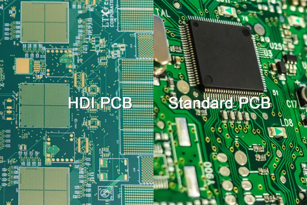
Laser drilling is a non-contact manufacturing process that uses a focused laser beam to create holes, or vias, in PCB materials. Unlike traditional mechanical drilling, which relies on physical bits to cut through layers, laser drilling offers unparalleled precision and control. This technology is critical for producing high-density interconnect (HDI) boards, which are essential for modern devices like smartphones, wearables, and IoT gadgets.
The primary reason laser drilling matters is its ability to create microvias—tiny holes with diameters as small as 50 micrometers (μm). These microvias allow for tighter component spacing, enabling PCB miniaturization while maintaining or even improving performance. For high-speed PCBs, where signal integrity is crucial, laser-drilled vias reduce signal loss and crosstalk, supporting data rates often exceeding 10 Gbps.
How Laser Drilling Works in PCB Manufacturing
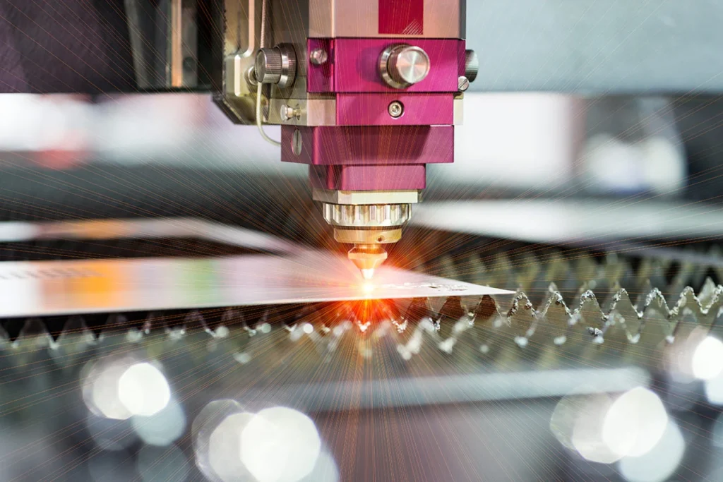
The laser drilling process involves directing a high-energy laser beam onto the PCB substrate to vaporize material and form holes. The beam’s intensity and focus are carefully controlled to ensure clean, precise cuts without damaging surrounding areas. There are two main types of lasers used in PCB production: CO2 lasers for larger holes and UV lasers for smaller, high-precision microvias.
Here’s a simplified breakdown of the laser drilling process:
- Setup: The PCB design file specifies the exact locations and sizes of vias. This data is programmed into the laser drilling machine.
- Material Removal: The laser targets specific spots, removing material layer by layer through ablation (vaporization).
- Cleaning: After drilling, residues are removed to ensure the vias are clean and ready for plating.
- Plating: The holes are coated with conductive material, typically copper, to establish electrical connections between layers.
This process is especially effective for multilayer boards, where precise via formation is needed to connect densely packed layers. With laser drilling, manufacturers can achieve aspect ratios (the ratio of hole depth to diameter) as high as 1:1, which is often impossible with mechanical methods.
Laser Drilling Advantages for PCB Miniaturization
One of the standout benefits of laser drilling is its role in PCB miniaturization. As devices shrink, so must the components and boards inside them. Here are the key ways laser drilling supports smaller designs:
- Microvia Precision: Laser drilling can create vias with diameters below 100 μm, far smaller than the 300 μm limit of mechanical drills. This allows for finer pitch components and denser layouts.
- Reduced Board Size: Smaller vias mean less space is needed for interconnections, enabling compact board designs without sacrificing functionality.
- Layer Stacking: Laser-drilled microvias facilitate HDI designs by allowing stacked vias, which connect multiple layers in a smaller footprint.
For example, in a typical smartphone PCB, laser drilling enables hundreds of microvias per square centimeter, supporting the integration of advanced chips and sensors in a device thinner than 8 mm.
Laser Drilling for High-Speed PCBs: Boosting Performance
High-speed PCBs are the backbone of applications like 5G networks, data centers, and automotive electronics, where signal integrity and speed are non-negotiable. Laser drilling plays a critical role in enhancing performance for these boards. Here’s how:
- Improved Signal Integrity: Laser-drilled vias have smoother walls and more precise geometries, reducing signal reflection and impedance mismatches. This is vital for maintaining signal integrity at frequencies above 1 GHz.
- Lower Crosstalk: Smaller, accurately placed vias minimize interference between adjacent signals, supporting data transfer rates of 25 Gbps or higher in advanced designs.
- Shorter Interconnects: Microvias enable shorter signal paths, reducing latency and power loss—key factors in high-speed applications.
For instance, in a server-grade PCB handling 10 Gbps data rates, laser-drilled vias can help maintain an impedance value of 50 ohms with minimal deviation, ensuring reliable performance under heavy loads.
High-Density Interconnect (HDI) and Via Formation with Laser Drilling
High-density interconnect technology is at the heart of modern PCB design, and laser drilling is the tool that makes it possible. HDI boards feature multiple layers of circuitry packed into a small area, relying on microvias for connections. Laser drilling excels in via formation for HDI designs due to its precision and flexibility.
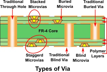
There are several types of vias used in HDI boards, all of which can be created with laser drilling:
- Blind Vias: These connect an outer layer to an inner layer without passing through the entire board, saving space.
- Buried Vias: Located entirely within internal layers, these vias free up surface space for components.
- Stacked Vias: Multiple vias are stacked on top of each other to connect several layers, a feat only achievable with laser precision.
Laser drilling ensures these vias are formed with exact alignment, often within a tolerance of ±10 μm. This accuracy is crucial for maintaining electrical performance in HDI boards, where even a slight misalignment can disrupt connectivity.
Additional Benefits of Laser Drilling in PCB Production
Beyond miniaturization and high-speed performance, laser drilling offers several other advantages that make it a preferred choice in PCB manufacturing:
- Material Versatility: Laser drilling works on a wide range of materials, including FR-4, polyimide, and even thin flexible substrates, without causing mechanical stress or cracks.
- Cost Efficiency for Complex Designs: While the initial setup for laser drilling equipment can be expensive, it reduces costs in high-volume production by minimizing errors and rework compared to mechanical drilling.
- Environmentally Friendly: Unlike mechanical drilling, laser drilling produces less waste and doesn’t require coolants or lubricants, making it a greener option.
- Scalability: Laser systems can easily adapt to different hole sizes and patterns by adjusting software settings, offering flexibility for custom designs.
These benefits make laser drilling not just a technical solution but also a strategic one for manufacturers aiming to stay competitive in the electronics industry.
Challenges and Considerations in Laser Drilling
While laser drilling offers numerous advantages, it’s important to acknowledge some challenges and considerations in its application:
- Initial Investment: Laser drilling machines are costly, often requiring significant upfront investment, which may be a barrier for smaller manufacturers.
- Material Limitations: Certain materials with high thermal conductivity or reflectivity can be harder to drill with lasers, requiring specialized equipment or settings.
- Process Complexity: Achieving optimal results demands precise control of laser parameters like power, pulse duration, and focus, which requires skilled operators and advanced software.
Despite these challenges, ongoing advancements in laser technology are continuously reducing costs and improving accessibility, making it a viable option for a growing number of PCB producers.
The Future of Laser Drilling in PCB Technology
As the electronics industry pushes toward even smaller and faster devices, laser drilling is poised to play an even larger role. Emerging trends like 5G, artificial intelligence, and the Internet of Things (IoT) are driving demand for HDI boards with unprecedented density and performance. Laser drilling technology is evolving to meet these needs with innovations such as:
- Ultra-Fast Lasers: Newer femtosecond lasers offer even higher precision and minimal heat damage, ideal for drilling vias smaller than 30 μm.
- Automation: Integration with AI and machine learning allows for real-time adjustments during drilling, improving accuracy and reducing production time.
- Hybrid Approaches: Combining laser and mechanical drilling for cost-effective solutions in mixed-design boards.
With the global market for laser drilling equipment projected to reach significant growth in the coming years, driven by the demand for miniaturized electronics, this technology will remain a cornerstone of PCB innovation.
Conclusion: Unlocking the Potential of Smaller, Faster PCBs with Laser Drilling
Laser drilling has revolutionized the way we design and manufacture PCBs, unlocking new possibilities for miniaturization, high-speed performance, and high-density interconnects. Its precision in via formation enables the creation of compact, powerful boards that power today’s most advanced electronics. From smartphones to data centers, the advantages of laser drilling are clear: smaller sizes, faster signals, and greater reliability.
For engineers and manufacturers, embracing laser drilling means staying ahead in a competitive industry where innovation is key. By leveraging this technology, you can achieve designs that meet the stringent demands of modern applications while optimizing production efficiency. As laser drilling continues to evolve, it will undoubtedly shape the future of PCB technology, making devices smaller, faster, and smarter than ever before.


