 ALLPCB


Are you new to PCB design and struggling with fitting components into tight spaces? Via-in-pad technology might be the solution you’re looking for. In this guide, we’ll break down what via-in-pad is, why it’s useful, and how to use it in your PCB layouts. Whether you’re searching for a via-in-pad tutorial, PCB layout for beginners, or a simple via-in-pad design approach, this post will walk you through the basics with clear, actionable steps to simplify complex designs.
What Is Via-in-Pad and Why Does It Matter?
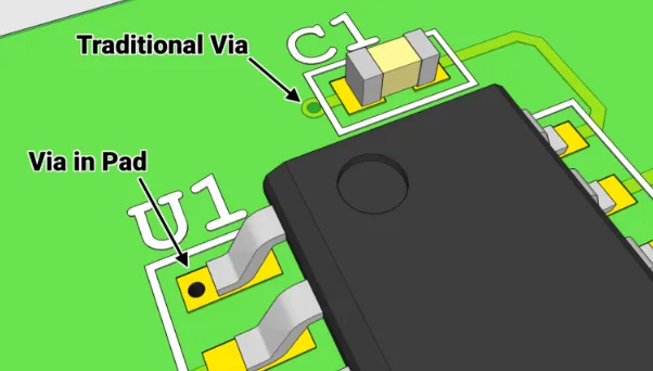
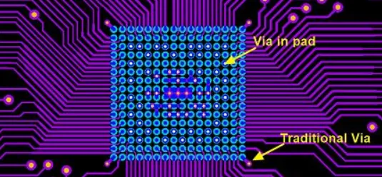
Via-in-pad is a PCB design technique where a via—a small hole that connects different layers of a circuit board—is placed directly inside a component’s pad. Unlike traditional vias that are placed outside pads and require additional routing space, via-in-pad saves room on the board. This method is especially helpful in modern electronics, where devices are getting smaller, and component density is increasing.
Why does this matter? As a beginner, you might notice that routing traces for high-density designs, like those with surface-mount devices (SMDs), can quickly become a puzzle. Via-in-pad helps by reducing the space needed for connections, allowing for tighter layouts without sacrificing functionality. It’s a game-changer for designs with fine-pitch components, such as ball grid arrays (BGAs), where pins are closely spaced, often less than 1 mm apart.
Benefits of Using Via-in-Pad in PCB Design
Before diving into the how-to, let’s explore why via-in-pad is worth considering for your next project. Here are some key advantages:
- Space Efficiency: By placing vias directly under component pads, you free up surface area for other traces or components. This is critical for compact designs like wearables or IoT devices.
- Improved Signal Integrity: Shorter trace lengths reduce signal delays and interference. For high-speed signals (e.g., above 1 GHz), this can lower impedance mismatches, ensuring better performance.
- Better Thermal Management: Vias under pads can act as thermal conduits, helping to dissipate heat from components like power ICs, which might otherwise overheat in dense layouts.
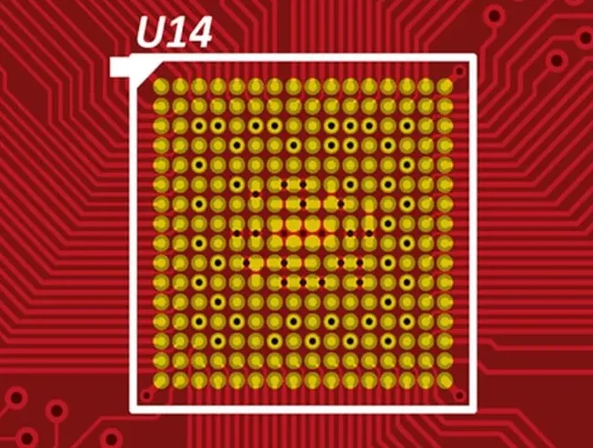
- Support for High-Density Components: Via-in-pad is often necessary for SMDs and BGAs with pitches as small as 0.5 mm, where traditional routing isn’t feasible.
While via-in-pad offers these benefits, it’s not without challenges, such as increased manufacturing complexity. We’ll cover how to address those later in this guide.
When Should You Use Via-in-Pad?
Not every PCB design needs via-in-pad. As a beginner, it’s important to know when this technique is the right fit. Consider using via-in-pad in these scenarios:
- Limited Board Space: If your design is constrained by size, such as in mobile devices or compact modules, via-in-pad can help you fit more components.
- High-Speed Circuits: For designs handling frequencies above 500 MHz, shorter connections via this method reduce signal loss and crosstalk.
- Fine-Pitch SMD Components: If you’re working with SMD via-in-pad designs, especially BGAs or QFNs with tight pin spacing, this approach is often the only way to route connections effectively.
On the flip side, for simpler designs with larger components and plenty of board space, traditional vias might be easier and more cost-effective to implement.
Basic PCB Routing: Understanding Vias First
Before jumping into via-in-pad specifics, let’s cover the basics of vias in PCB routing. A via is a plated-through hole that connects different layers of a multi-layer PCB. For example, a signal might start on the top layer, pass through a via to the bottom layer, and connect to another component. Standard vias are placed away from pads and require traces to link them to components, taking up extra space.
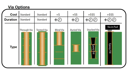
There are three main types of vias:
- Through-Hole Vias: These go through all layers of the board and are the most common type.
- Blind Vias: These connect an outer layer to an inner layer but don’t go through the entire board.
- Buried Vias: These connect inner layers only and aren’t visible from the outside.
Via-in-pad typically uses through-hole or blind vias, placed directly under a component’s pad. This eliminates the need for extra traces, streamlining your layout. As a beginner learning PCB layout, mastering basic via placement will help you transition to advanced techniques like via-in-pad.
Simple Via-in-Pad Design: Step-by-Step Tutorial
Now that you understand the basics, let’s walk through a via-in-pad tutorial tailored for beginners. Follow these steps to incorporate this technique into your PCB layout:
Step 1: Plan Your Layout
Start by identifying components that need via-in-pad, such as fine-pitch SMDs or BGAs. Use your schematic to map out where signals need to go between layers. Planning ahead prevents unnecessary vias and keeps your design clean. For instance, if a BGA has 100 pins with a 0.8 mm pitch, you’ll likely need vias under most pads to route signals to inner layers.
Step 2: Choose the Right Via Size
Via size matters. For via-in-pad, smaller is often better, but it depends on manufacturing capabilities. A typical via diameter might be 0.2 mm to 0.3 mm with a drill size of 0.1 mm to 0.15 mm. Check with your PCB fabricator for their minimum via size and annular ring requirements (the copper ring around the via). Too small, and it might not be reliable; too large, and it won’t fit under the pad.
Step 3: Place the Via Under the Pad
In your PCB design software, place the via directly under the component pad. Ensure the via is centered to avoid soldering issues. Most modern design tools allow you to drag and drop vias into pads, automatically adjusting the layout. If the pad is for an SMD component, confirm that the via doesn’t interfere with solder paste application.
Step 4: Use Via Filling or Capping (If Needed)
One challenge with via-in-pad is that an open via can cause solder to wick away during assembly, leading to poor connections. To prevent this, consider via filling (plugging the via with non-conductive material) or capping (covering it with a thin layer of copper). Filled vias are common for high-reliability designs, while capped vias work for less critical applications. Note that filling or capping can increase costs, so weigh the trade-offs.
Step 5: Route Traces on Other Layers
Once the via is in place, route the connected traces on the appropriate inner or outer layers. Keep trace lengths as short as possible to maintain signal integrity, especially for high-speed designs. For example, a 5 GHz signal can experience significant loss over just a few millimeters of extra trace length, so optimize your routing.
Step 6: Verify Design Rules
Run a design rule check (DRC) in your software to ensure the via-in-pad meets spacing, clearance, and manufacturing constraints. Common issues include vias too close to other features or pads not large enough to accommodate the via. Fix any errors before finalizing your design.
Challenges and Solutions in Via-in-Pad Design
While via-in-pad is powerful, it comes with hurdles, especially for beginners. Here’s how to tackle common issues:
- Solder Wicking: As mentioned, solder can flow into an open via during reflow, causing weak joints. Solution: Use filled or capped vias, or tent the via with solder mask if filling isn’t an option.
- Manufacturing Costs: Via-in-pad often requires advanced fabrication processes, increasing costs. Solution: Reserve this technique for areas where it’s absolutely necessary, like under BGAs, and use traditional vias elsewhere.
- Signal Integrity Risks: Poorly placed vias can introduce noise or reflections in high-speed circuits. Solution: Simulate your design if possible, or follow best practices like keeping vias away from critical signal paths unless unavoidable.
Tips for SMD Via-in-Pad Design
Working with surface-mount devices (SMDs) often means dealing with tight spaces, making via-in-pad a go-to technique. Here’s a quick SMD via-in-pad guide for beginners:
- Match Pad and Via Sizes: Ensure the pad is large enough to accommodate the via without compromising solderability. A pad diameter of at least 0.5 mm larger than the via is a good starting point.
- Avoid Overcrowding: Don’t place vias under every SMD pad unless necessary. Prioritize critical connections to reduce manufacturing complexity.
- Test Assembly Early: If possible, prototype your design to check for soldering issues. SMD components are sensitive to via placement, and early testing can save headaches later.
Best Practices for PCB Layout for Beginners
As you integrate via-in-pad into your designs, keep these general PCB layout tips in mind to ensure success:
- Start Simple: Begin with basic designs before tackling high-density layouts. Practice traditional via placement first to build confidence.
- Use Grid Systems: Align components and vias on a grid in your design software. This keeps your layout organized and easier to route.
- Minimize Layer Count: While via-in-pad often requires multi-layer boards, don’t add unnecessary layers. A 4-layer board is often enough for most beginner projects.
- Collaborate with Fabricators: Early communication with your PCB manufacturer can clarify via-in-pad capabilities and constraints, avoiding costly redesigns.
Conclusion: Mastering Via-in-Pad for Better PCB Designs
Via-in-pad is a powerful tool for simplifying complex PCB layouts, especially when space is tight or you’re working with high-density components like SMDs and BGAs. By following this beginner-friendly guide, you’ve learned the basics of via-in-pad design, from understanding its benefits to implementing it step by step in your projects. Remember to plan carefully, choose the right via sizes, and address challenges like solder wicking with practical solutions.
As you grow in your PCB design journey, via-in-pad will become second nature, helping you tackle even the most demanding layouts with confidence. Keep practicing basic PCB routing, experiment with simple via-in-pad designs, and soon, you’ll be creating compact, efficient boards that meet modern electronics’ demands.


