 ALLPCB


In the world of electronics manufacturing, the reliability of printed circuit boards (PCBs) hinges on the quality of solder joints. But how can manufacturers ensure these tiny connections are flawless, especially when they’re hidden beneath components like Ball Grid Arrays (BGAs)? The answer lies in advanced techniques like X-ray inspection. This powerful tool helps detect defects such as voids and poor connections, ensuring the durability and performance of electronic devices. In this blog, we’ll dive deep into the importance of solder joint X-ray analysis, the specifics of BGA solder joint inspection, and the critical role of void detection in solder, offering practical insights for engineers and manufacturers.
Why Solder Joint Reliability Matters in PCB Manufacturing
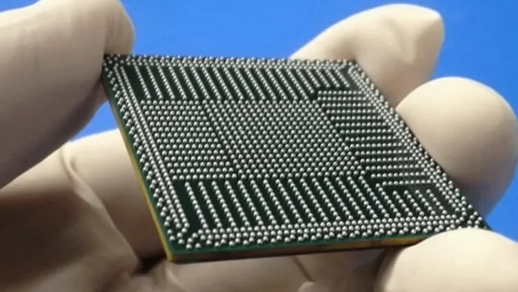
Solder joints are the backbone of any PCB, forming the electrical and mechanical connections between components and the board. A single faulty joint can lead to device failure, reduced performance, or even safety hazards. This is especially true for high-density components like BGAs, where hundreds of tiny solder balls are hidden beneath the package, making visual inspection impossible.
Reliability issues in solder joints often stem from defects like voids (air pockets within the solder), insufficient wetting, or cracks. These flaws can weaken the joint, disrupt electrical conductivity, or cause thermal stress over time. For industries like aerospace, automotive, and medical devices, where failure is not an option, ensuring solder joint integrity is non-negotiable. This is where X-ray inspection becomes a game-changer, allowing manufacturers to see inside these hidden connections and catch defects early.
What Is X-Ray Inspection for PCB Solder Joints?
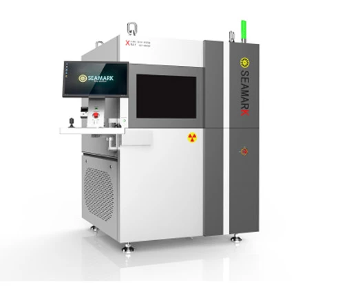
X-ray inspection is a non-destructive testing method that uses high-energy X-rays to penetrate materials and create detailed images of a PCB’s internal structure. Unlike visual or optical inspection, which can only assess surface-level features, X-ray systems reveal what’s happening inside solder joints, even under densely packed components. This technology is particularly vital for modern electronics, where miniaturization and complex designs make traditional inspection methods inadequate.
In practice, an X-ray machine captures images of the PCB from multiple angles, allowing engineers to analyze the shape, size, and quality of solder joints. For instance, in BGA solder joint inspection, X-ray images can show whether the solder balls are uniformly formed or if defects like voids are present. This level of detail helps manufacturers address issues before they escalate into costly failures.
The Role of Solder Joint X-Ray Analysis in Quality Control
Solder joint X-ray analysis is a cornerstone of quality control in PCB manufacturing. By providing a clear view of internal connections, it helps identify a range of defects that could compromise reliability. Here are some key benefits of this technique:
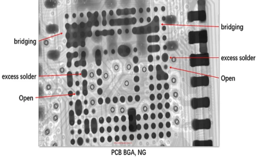
- Detecting Hidden Defects: X-ray analysis can spot issues like insufficient solder, bridging, or misalignment in hidden joints, which are common in BGAs and other surface-mount components.
- Ensuring Consistency: It allows manufacturers to verify that every joint meets design specifications, maintaining uniformity across production batches.
- Preventing Failures: Early detection of defects reduces the risk of field failures, saving time and resources in the long run.
For example, in a high-reliability application like an automotive control unit, even a small defect in a solder joint could lead to a malfunction. X-ray analysis ensures that such risks are minimized by catching problems during the manufacturing stage.
BGA Solder Joint Inspection: Challenges and Solutions
Ball Grid Array (BGA) components are widely used in modern electronics due to their high pin density and compact size. However, inspecting BGA solder joints poses unique challenges. Since the solder balls are located beneath the component, visual inspection is impossible, and even automated optical inspection (AOI) systems fall short. This is where X-ray inspection shines, offering a reliable solution for assessing these hidden connections.
During BGA solder joint inspection, X-ray systems can evaluate several critical factors:
- Solder Ball Shape and Size: Uniformity in the shape and diameter of solder balls (typically ranging from 0.3mm to 0.76mm, depending on the BGA type) indicates a proper connection.
- Alignment: Misaligned components can lead to open circuits or shorts, which X-ray images can easily detect.
- Joint Integrity: The presence of cracks or incomplete reflow can be identified, ensuring the joint can withstand mechanical and thermal stress.
By addressing these issues early, manufacturers can avoid costly rework and ensure that BGA components perform reliably over their lifespan. For instance, in a consumer electronics device, a poorly soldered BGA could cause intermittent failures, leading to customer dissatisfaction. X-ray inspection helps prevent such scenarios by ensuring every joint is up to standard.
Void Detection in Solder: Why It’s Critical
One of the most common defects in solder joints is the presence of voids—empty spaces or air pockets trapped within the solder. While small voids (less than 10% of the joint area) may not immediately affect performance, larger voids can weaken the joint, reduce thermal conductivity, and increase the risk of failure under stress. This is especially concerning in high-power applications, where heat dissipation is critical.
Void detection in solder is a primary focus of X-ray inspection. Using high-resolution imaging, manufacturers can measure the size and location of voids within a joint. Industry standards, such as those from the Institute of Printed Circuits (IPC), often specify acceptable void percentages—typically below 25% for BGA solder balls in Class 2 assemblies (general electronics) and even stricter limits for Class 3 (high-reliability applications).
For example, in a power supply board, excessive voiding in solder joints could lead to overheating and eventual failure. X-ray inspection allows engineers to quantify voiding and take corrective actions, such as adjusting reflow profiles or using vacuum soldering techniques to minimize air entrapment during the soldering process.
How X-Ray Inspection Works: A Step-by-Step Overview
Understanding the X-ray inspection process can help manufacturers integrate it effectively into their workflows. Here’s a simplified breakdown of how it works:
- Setup: The PCB is placed in an X-ray machine, which is calibrated to the appropriate energy level for penetrating the board’s materials without damaging components.
- Imaging: X-rays pass through the PCB, and a detector captures the resulting image. Dense materials like solder absorb more X-rays, appearing darker, while voids or less dense areas appear lighter.
- Analysis: Engineers or automated software analyze the images to identify defects. Modern systems often use algorithms to quantify void percentages or flag anomalies.
- Reporting: Results are compiled into a report, highlighting any issues and recommending corrective actions.
This process is fast, often taking just a few minutes per board, and can be integrated into high-volume production lines for real-time quality control. For instance, a manufacturer producing thousands of smartphone boards daily can use X-ray inspection to sample batches, ensuring consistent quality without slowing down production.
Benefits of X-Ray Inspection for PCB Reliability
Investing in X-ray inspection offers several advantages for PCB manufacturers focused on reliability:
- Non-Destructive Testing: Unlike cross-sectioning or other destructive methods, X-ray inspection evaluates solder joints without damaging the board.
- High Accuracy: Modern X-ray systems provide resolution down to a few micrometers, allowing precise defect detection.
- Versatility: Beyond solder joints, X-ray inspection can assess other internal features, such as vias in multilayer boards or wire bonds in packaged components.
These benefits translate into tangible results. For example, a study in the electronics industry found that implementing X-ray inspection reduced field failure rates by up to 30% for high-density assemblies, proving its value in ensuring long-term reliability.
Best Practices for Implementing X-Ray Inspection
To maximize the effectiveness of X-ray inspection, manufacturers should follow these best practices:
- Train Staff: Ensure operators are skilled in interpreting X-ray images and understanding defect criteria, as human judgment often plays a role alongside automated analysis.
- Calibrate Equipment: Regularly calibrate X-ray machines to maintain accuracy, as variations in energy levels can affect image quality.
- Set Clear Standards: Define acceptable limits for defects like voiding based on industry standards (e.g., IPC-A-610) and application requirements.
- Integrate with Other Methods: Combine X-ray inspection with techniques like automated optical inspection (AOI) for a comprehensive quality control strategy.
By adopting these practices, manufacturers can build a robust inspection process that minimizes defects and maximizes PCB reliability.
Future Trends in Solder Joint Inspection Technology
As electronics continue to evolve, so does the technology for inspecting solder joints. Emerging trends in X-ray inspection include:
- 3D X-Ray Imaging: Also known as computed tomography (CT), this technique creates three-dimensional models of solder joints, offering even greater detail than traditional 2D X-rays.
- Artificial Intelligence (AI): AI-powered software can analyze X-ray images faster and more accurately than humans, identifying subtle defects with minimal oversight.
- Inline Integration: Advances in automation are making it easier to integrate X-ray systems directly into production lines for real-time inspection without slowing down manufacturing.
These innovations promise to make solder joint inspection more efficient and effective, ensuring that even the most complex PCB designs meet the highest reliability standards.
Conclusion: Building Trust Through Reliable Solder Joints
In the fast-paced world of electronics manufacturing, the reliability of solder joints can make or break a product. X-ray inspection offers a powerful solution for ensuring the quality of these critical connections, especially in challenging areas like BGA components. Through solder joint X-ray analysis, BGA solder joint inspection, and void detection in solder, manufacturers can catch defects early, prevent failures, and deliver products that meet the highest standards of performance and durability.
By embracing this technology and following best practices, companies can build trust with their customers and stay ahead in a competitive market. Whether you’re producing consumer gadgets or life-critical medical devices, X-ray inspection is an essential tool for guaranteeing the integrity of every PCB. With ongoing advancements in imaging and automation, the future of solder joint reliability looks brighter than ever.


