ALLPCB


Overview
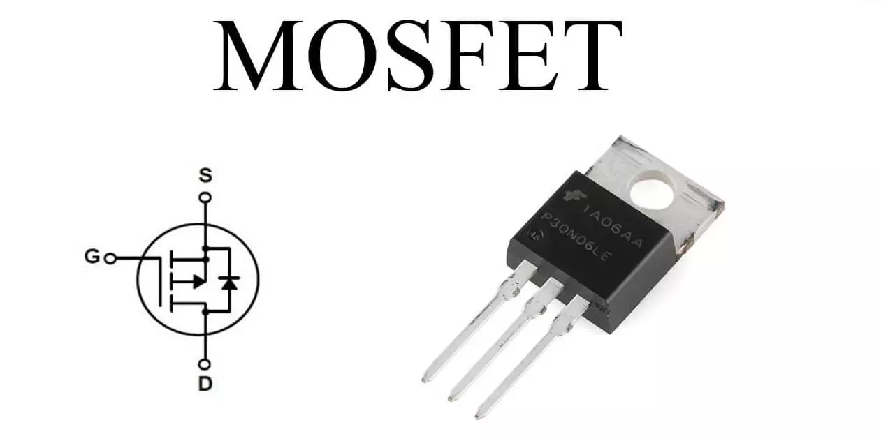
Source, Drain and Gate correspond to the three terminals of a field-effect transistor: source (S), drain (D) and gate (G). This article focuses on drain-voltage-related breakdowns and device heating, not gate-oxide breakdown.
MOSFET breakdown pathways
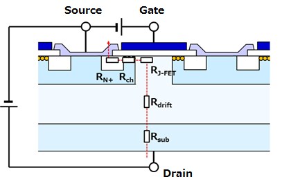
With source, gate and substrate tied to ground while sweeping the drain voltage until the drain current reaches about 1 uA, there are three leakage/breakdown channels from the drain: drain-to-source, drain-to-bulk, and drain-to-gate.
1. Drain-to-source punch-through
Punch-through occurs when a reverse bias on the drain expands the drain/bulk PN-junction depletion region until it reaches the source, creating a conductive path between source and drain without forming a channel. To prevent punch-through you must consider the PN junction reverse-bias characteristics: depletion width depends on voltage and on the doping concentrations on both sides. Higher doping suppresses depletion extension.
In the process flow there is typically an anti-punch-through implant (APT). The implant type should match the well type. In practice, when a wafer acceptance test (WAT) shows degraded breakdown voltage and the leakage is originating from the source side, also check poly CD, spacer width or LDD implant issues. To diagnose, verify whether both NMOS and PMOS fail and use poly-related WAT checks for poly CD variations.
Characteristics of punch-through:
- Soft breakdown point: current increases progressively during breakdown because the depletion region extends and produces large current.
- Soft breakdown occurs when source and drain depletion regions meet; carriers injected from the source are accelerated through the depletion field to the drain.
- Punch-through is generally non-destructive.
- It typically occurs in the channel body rather than at the channel surface.
- Edge regions (bird’s beak) have higher doping than the channel center, so punch-through usually happens in the middle of the channel.
- Poly gate length affects punch-through: longer gate length tends to increase punch-through.
2. Drain-to-bulk avalanche breakdown
This is conventional PN-junction avalanche breakdown. A large reverse bias at the drain widens the depletion region and increases the electric field. High-energy carriers create electron-hole pairs by impact ionization; these carriers then generate additional pairs in an avalanche process, causing a rapid current rise and potentially destructive heating.
To improve junction breakdown voltage (BV), reduce the peak electric field in the depletion region. Since lowering operating voltage is not always possible, designers change the doping profile to widen the depletion region. Abrupt junctions have lower breakdown voltage than graded junctions. Doping concentration also matters: higher doping produces a narrower depletion width and stronger electric field, which reduces BV. The lower-doped side typically dominates the breakdown voltage because its depletion region is larger. A simple approximation is BV = K*(1/Na + 1/Nb); if Na and Nb differ by an order of magnitude, the smaller term dominates. If process monitoring shows reduced BV originating from the junction, investigate the source/drain implant profiles.
3. Drain-to-gate breakdown
Drain-to-gate breakdown is caused by overlap between drain and gate that stresses the gate oxide, similar to gate-oxide breakdown. This failure mode is sensitive to poly profile and sidewall damage, and it can be aggravated by gate-induced drain leakage (GIDL), which increases leakage and effectively lowers the observed BV. In practice, the first two channels account for most BV failures.
Related Reading: Understanding MOSFET Parameters
On-state breakdown
The above discussions assume the transistor is off (gate at 0 V). Applying an excessive drain voltage while the gate is on can also cause breakdown; this is called on-state breakdown and is observed more often in NMOS devices at low gate overdrive or during device turn-on. It is common to test BV in the on-state (BVON) as well.
Causes of heating in low-current MOSFETs
MOSFETs are widely used as switches in power and driver circuits. Although RDS(on) is the standard datasheet parameter for conduction resistance, devices that remain in conduction for long periods can heat up. Junction temperature rise in turn increases RDS(on), creating a positive feedback.
Common reasons for significant heating at relatively low currents:
- Circuit design forcing the MOSFET to operate in the linear region instead of as a switch.
- Excessive switching frequency to meet size constraints, increasing switching losses.
- Insufficient thermal design: even with ID lower than the device maximum, poor heat dissipation can cause large temperature rise; external heatsinking may be required.
- Incorrect device selection: underestimating power dissipation or neglecting the effective on-resistance under operating conditions.
Mitigations for MOSFET heating
- Implement adequate thermal design and use sufficient heatsinking or thermal vias.
- Use thermally conductive adhesive or thermal interface material to improve heat transfer.
Using MOSFETs for reverse-polarity protection
Reverse connection of the supply can damage circuits. A classic protection method is a series diode, but its forward voltage drop wastes power. Using a MOSFET in series provides near-zero voltage drop when oriented correctly, because modern MOSFETs can have milliohms of RDS(on). For example, a 6.5 mΩ device at 1 A drops only 6.5 mV.
NMOS reverse-polarity protection
When connected correctly: at power-up the MOSFET's body diode conducts, so the source sits about 0.6 V above ground. The gate is at battery voltage, so VGS ≈ VBAT - 0.6 V which exceeds the threshold and turns the MOSFET on. The MOSFET then conducts with very low RDS(on), effectively shorting out the body diode and reducing the drop to nearly zero.
When the supply is reversed: VGS = 0 so the MOSFET remains off and the load is disconnected, protecting the circuit.
PMOS reverse-polarity protection
When connected correctly: at power-up the body diode conducts, the source sits at VBAT - 0.6 V while the gate is at ground, turning the PMOS on. The current from drain to source shorts the diode and reduces the forward drop.
When the supply is reversed: the gate is high and the PMOS remains off, protecting the circuit.
Related Reading: PMOS Reverse-Protection Circuit Design
Connection guidance
Place NMOS devices with their drain-source path in series on the negative rail, PMOS on the positive rail, so that the body diode conducts only in the correct polarity. Note that the apparent DS current direction in these protection schemes is reversed compared with the typical switching direction; MOSFETs allow source and drain interchangeability in many applications, unlike BJTs.
MOSFET power-loss measurement
Measuring switching losses of MOSFETs or IGBTs is essential for power-supply tuning. Switching losses primarily occur during the turn-on and turn-off transitions; conduction losses during the on-state are usually smaller and steady. Accurate loss measurement requires capturing voltage and current waveforms during transitions.
Measurement practice
A typical loss-measurement setup monitors drain voltage and drain current while calculating instantaneous power. For standard MOSFETs with repeatable period-to-period waveforms, measuring one representative period is often sufficient. For PFC MOSFETs, voltage and current waveforms vary from cycle to cycle, so accurate evaluation requires longer capture durations (typically >10 ms), high sampling rates (recommended 1 GS/s), large memory depth (recommended >10 M points) and use of all raw samples (no subsampling) in the power calculation.
Summary
This article reviewed the main drain-related breakdown mechanisms, common causes of heating in MOSFETs even at modest currents, practical mitigations, reverse-polarity protection techniques using MOSFETs, and key considerations for power-loss measurement. These points can guide device selection, process troubleshooting and circuit-level thermal and reliability design.