ALLPCB


1. Introduction
In circuit designs, different chips often use different supply voltages, such as 1.8V, 3.3V, and 5V. To enable communication between devices that use different signal levels, level shifting is required. This article describes several common level-shifting methods.
2. Diode level shifting
Typical application: pull-up resistor plus diode
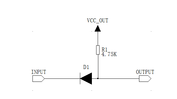
Applicable scenario: converting a lower-voltage output to a higher-voltage input (input signal level higher than output device's native level)
Advantages: low cost, few components
Disadvantages: unidirectional only; diode introduces a voltage drop, so the input signal must be higher than the output device's required level
Component selection: choose a low-forward-voltage diode such as a Schottky diode to minimize voltage drop and avoid incorrect logic-level detection.
Operation:
When the 3.3V device outputs a high level, the pull-up to 5V pulls the input device toward 5V through the diode.
When the 3.3V device outputs a low level, it pulls the OUTPUT low, pulling the input device low as well.
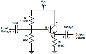
3. Bipolar transistor level shifting
Basic application circuit:

Applicable scenario: converting a lower-voltage output to a higher-voltage input
Advantages: low cost, few components; compared with a diode, a bipolar transistor requires less drive current at the input, which can be advantageous for peripherals with limited drive capability
Disadvantages: unidirectional only; there is VCE or VBE drop due to PN junctions
Component selection: choose transistors with low saturation or junction voltage to reduce voltage loss.
Operation:
When the 3.3V device outputs a high level, the pull-up to 5V pulls the input device toward 5V.
When the 3.3V device outputs a low level, the transistor conducts and pulls the input device low.
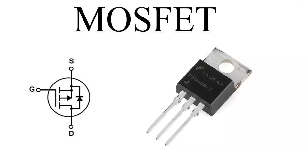
4. MOSFET-based level shifting
Applicable scenario: suitable for most level-shifting requirements
Advantages: can be bidirectional, low on-resistance resulting in small voltage drop, and capable of high-speed operation
The following analyzes operation for one I2C signal line:
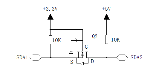
When SDA1 (3.3V side) outputs high: Vgs of Q1 = 0, Q1 is off, and SDA2 is pulled up to 5V by R3.
When SDA1 outputs low: Vgs of Q1 ≈ 3.3V, exceeding the threshold, so Q1 turns on and pulls SDA2 low through the MOSFET.
When SDA2 (5V side) outputs high: Vgs of Q1 remains 0, Q1 stays off, and SDA1 is pulled up to 3.3V by R2.
When SDA2 outputs low: the MOSFET's intrinsic body diode initially conducts, pulling SDA1 low; then Vgs ≈ 3.3V causes Q1 to turn on, further pulling SDA1 down. This mechanism enables bidirectional level translation for open-drain buses like I2C.
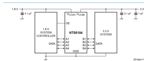
5. Dedicated level-shifter ICs
If the application requires higher switching frequencies or minimal voltage drop, many manufacturers offer dedicated level-shifter ICs.
Example device characteristics:
Voltage ranges: VCC(A): 1.65 V to 3.6 V; VCC(B): 2.3 V to 5.5 V
Maximum data rate: 50 Mbps
Multiple package options
Channels: 4
Typical use cases: I2C, UART, GPIO, etc.
Typical application diagram:
6. Conclusion
There are many level-shifting methods and circuits; choose the appropriate solution based on system requirements. Dedicated level-shifter ICs are mature and suitable for the majority of use cases.