ALLPCB


Introduction
Limited and shrinking PCB space, tight development schedules, and stringent electromagnetic interference (EMI) standards such as CISPR 32 and CISPR 25 make it difficult to achieve power supplies that deliver high efficiency and good thermal performance. Power supply design is often pushed toward the end of the overall design cycle, forcing designers to fit complex power systems into ever smaller areas. That frequently leads to compromises on performance and passes issues to test and verification stages. The three goals of simplicity, high performance, and small solution size often conflict, so teams tend to prioritize one or two at the expense of the third, especially under schedule pressure. These tradeoffs are common but avoidable with careful design choices.
This article summarizes EMI issues caused by power supplies in complex electronic systems and describes common mitigation strategies. It outlines methods to reduce EMI while maintaining efficiency and fitting power circuitry into constrained solution spaces.
What Is EMI?
Electromagnetic interference is an electromagnetic signal that degrades system performance. It couples into circuits via magnetic induction, electrostatic coupling, or conduction. EMI is a critical design challenge for automotive, medical, and test-and-measurement equipment. Constraints such as higher power density, increased switching frequency, and larger currents tend to worsen EMI, so mitigation techniques are needed early to avoid schedule delays due to failing EMI compliance tests.
Types of EMI Coupling
EMI arises when a noise source and a susceptible receiver within an electronic system become coupled. EMI coupling is commonly classified by the coupling medium: conducted or radiated.
Conducted EMI (low frequency, roughly 450 kHz to 30 MHz) couples into components via parasitic impedances and power or ground connections. Conducted noise can be split into common-mode and differential-mode noise.
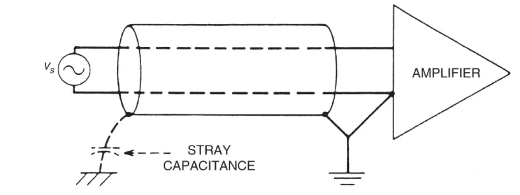
Common-mode noise is conducted through parasitic capacitance and high dV/dt (C × dV/dt). It travels via parasitic capacitances along paths from either signal polarity to ground, as shown in Figure 1.
Differential-mode noise is conducted via parasitic inductance (magnetic coupling) and high di/dt (L × di/dt).
Figure 1. Differential-mode and common-mode noise.
Radiated EMI (higher frequency, roughly 30 MHz to 1 GHz) transfers noise wirelessly via magnetic field energy to nearby devices. In switching power supplies, this noise is the result of high di/dt coupling with parasitic inductances. Radiated noise can affect adjacent components.
EMI Control Techniques
The first step in addressing EMI is identifying it as a problem. This requires quantifying the electromagnetic energy produced by the power supply, typically using an EMI test chamber. Once testing confirms EMI issues, designers usually apply several traditional corrective strategies:
- Achieve high efficiency within constrained PCB space.
- Maintain good thermal performance.
- Layout optimization: careful power-layout and component selection are important. Successful layouts depend heavily on the designer's experience. Layout optimization is iterative, and experienced power designers can reduce the number of iterations. Lack of in-house experience can lengthen the process.
- Snubbers: allocating board space for simple snubber circuits (for example, an RC filter from the switching node to ground) can suppress switching-node ringing, a contributor to EMI. However, snubbers add losses and can reduce efficiency.
- Slowing edge rates: reducing gate-drive slew rate can also reduce switching-node ringing, but, like snubbers, this typically reduces overall system efficiency.
- Spread-spectrum frequency modulation (SSFM): modulating the clock that drives the switching frequency within a specified range (for example, ±10% of the programmed switching frequency) spreads peak noise energy across a wider frequency band, reducing narrowband peaks.
- Filters and shielding: effective but often costly and area-consuming, and they can complicate manufacturing.
All of the above measures can reduce noise but have tradeoffs. Reducing noise at the source in the regulator is an effective approach because it can minimize the need for extensive filtering, shielding, or layout rework.
Minimize High?di/dt Current Loops
To reduce EMI, it is essential to identify and minimize high di/dt current loops in the power circuit, often called hot loops. In a typical buck converter switching cycle, when M1 is off and M2 is on, AC current flows along one loop; when M1 is on and M2 is off, current flows along another loop. The loop that conducts the full-switched AC current (switching from zero to IPEAK and back to zero) is the hot loop because it has the largest AC and EMI energy.
High di/dt and parasitic inductance in the hot loop produce electromagnetic noise and switching ringing. To reduce EMI and improve performance, the radiated effects of the hot loop should be minimized. Electromagnetic emissions from the hot loop increase with loop area. Therefore, reducing the PCB area of the hot loop and using low-impedance decoupling capacitors placed as close as possible to the switching nodes reduces emissions.
Local Field Cancellation and Package Techniques
Although it is impossible to eliminate the hot-loop area entirely, the hot loop can be split into two adjacent loops with opposite polarity. When implemented correctly, these opposing loops form local magnetic fields that cancel each other at short distances. This field-cancellation concept is the basis for regulator designs that emphasize low emitted magnetic fields.
Another way to improve EMI performance is to shorten conductors in the hot loop. Replacing traditional bond-wire connections between the die and package pins with flipped-die packaging and copper pillars reduces the distance between internal FETs, package pins, and input capacitors, thereby shrinking the hot-loop area and lowering emissions.
Integrated Low?Noise Regulator Implementations
Some regulator designs incorporate layout and package techniques to reduce EMI sensitivity to PCB layout. Integrating input capacitors and other critical passive components into the package can place these components as close as possible to the pins, keeping hot loops and ground returns within the package and minimizing PCB loop area. Such approaches also reduce PCB area and layout sensitivity.
Package-level improvements can also improve thermal performance. Large exposed ground pads on a package enable better heat transfer into the PCB, and eliminating high-resistance bond wires can improve conversion efficiency. When tested under EMI compliance, certain low-noise switching regulator implementations can meet stringent automotive standards with margin.
μModule Low?Noise Regulators
Combining low-noise regulator design techniques with μModule packaging yields power products that are easier to design with while meeting thermal, reliability, accuracy, efficiency, and EMI requirements. For example, an integrated μModule can include two input capacitors arranged to achieve magnetic field cancellation along with other required passives inside a compact BGA package, simplifying PCB design and placement.
Powering Noise?Sensitive ADCs Without an LDO
High-speed ADCs often require several rails, some of which must be very low noise to achieve peak ADC performance. A common compromise is to use a switching regulator followed by a low-noise LDO. The switching regulator provides efficient bulk conversion, while the LDO suppresses switching noise. Minimizing the LDO drop helps retain efficiency, but multiple regulators increase layout complexity and can introduce thermal challenges at higher loads.
Newer low-noise μModule switching regulators can provide the low-noise performance needed by ADCs without an LDO in some cases. These μModules combine low-noise switching topology with integrated packaging to reduce board area and sensitivity to layout. They can also be used with additional output LC filtering if further noise reduction is required. Comparative tests have shown that in certain configurations, a properly implemented μModule regulator can drive an ADC directly without measurable degradation in SFDR or SNDR compared with a switching-plus-LDO approach.
The primary benefit of such an implementation is a reduction in component count, improved efficiency, simplified manufacturing, and reduced PCB area.
Conclusion
As system designs must meet increasingly strict EMI requirements, modular and package-aware power designs become important, particularly where in-house power-design expertise is limited. Applying low-emission regulator techniques in compact packages reduces layout sensitivity and can shorten time to market while conserving PCB space.
Advantages of Low?Noise μModule Regulators
- Reduces PCB layout iteration time for noise issues.
- Eliminates or reduces the need for external EMI filters, saving components and board area.
- Lowers the need for in-house power-noise debugging expertise.
- Offers high efficiency across a wide operating frequency range.
- May eliminate the need for LDO post-regulation for noise-sensitive devices.
- Shortens design cycles.
- Enables high efficiency in compact PCB areas.