ALLPCB


Introduction
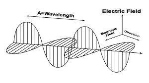
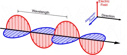
Electromagnetic radiation refers to energy waves that propagate through space. Familiar examples include radio, microwave, light, and X-rays, which are electromagnetic radiation at different frequencies. Visible light is only a small part of the spectrum, roughly 400–700 THz. Radio waves occupy the kHz to GHz range, covering systems such as WiFi, Bluetooth, mobile-phone communication, satellite links, and FM broadcast.
While radio and wireless communication are useful, electronic devices can also produce unintended radiation that interferes with other devices or with intended communications. EMPs and deliberate radio jammers are extreme examples, but for typical electronics the concern is EMI (electromagnetic interference) and EMC (electromagnetic compatibility). EMI refers to unintended emissions from a device that may disturb others. EMC refers to how a device behaves in the presence of electromagnetic disturbance. Most electronic systems operate with clock rates in the kHz, MHz, and GHz ranges, so emitted energy in the radio spectrum is the primary EMI/EMC concern.
Product Certification
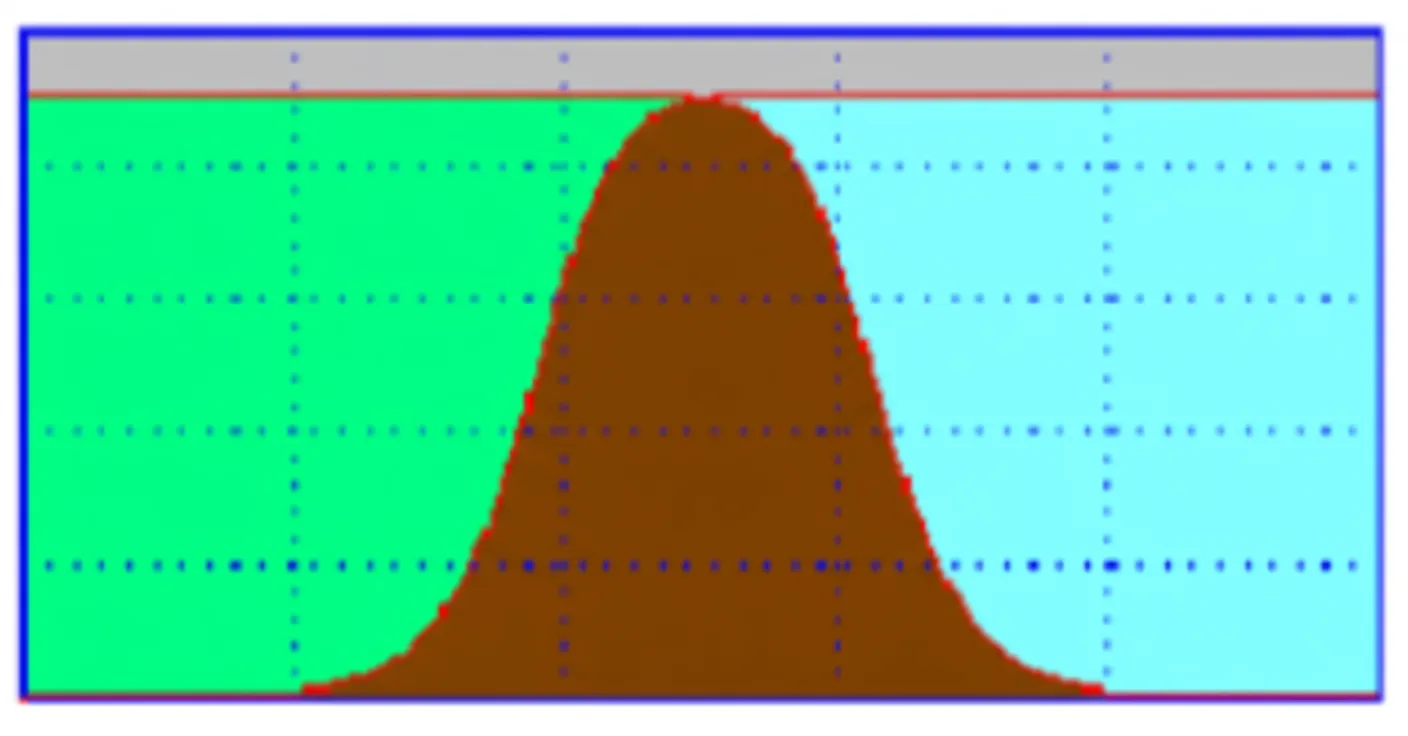
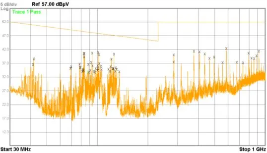
Products sold in some markets must pass EMI/EMC testing performed by accredited labs. A radiated emission test result is typically shown as a plot of amplitude versus frequency, where the device pass/fail limit is indicated by a threshold line:
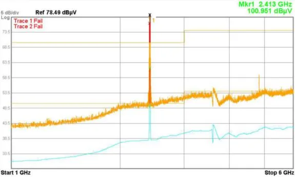
If emissions exceed the specified limits, the device will fail the test:
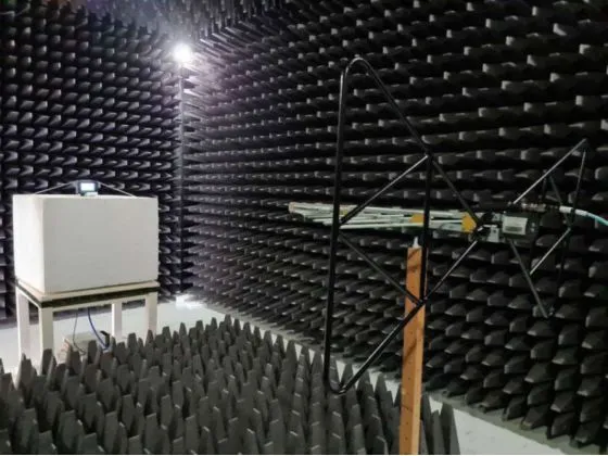
Tests are performed under standardized conditions in shielded chambers. An antenna receives radiation from the device and a spectrum analyzer plots it:
Design Goals for EMC
Designing for EMC is, in effect, the opposite of designing a radio. We want to ensure our device is not functioning as an unintended transmitter, except where it is purposely a radio (for example, a WiFi radio). Antennas both radiate when driven and generate voltages/currents when exposed to fields, so traces and conductors that behave like antennas must be controlled.
Electromagnetic radiation is produced when charged particles accelerate, which happens when currents change direction or switch on and off. EMI/EMC design therefore focuses on the system's AC (switching voltage/current) elements and any conductors that can act as antennas. In practice, applying sound high-speed design techniques will also improve EMI/EMC performance.
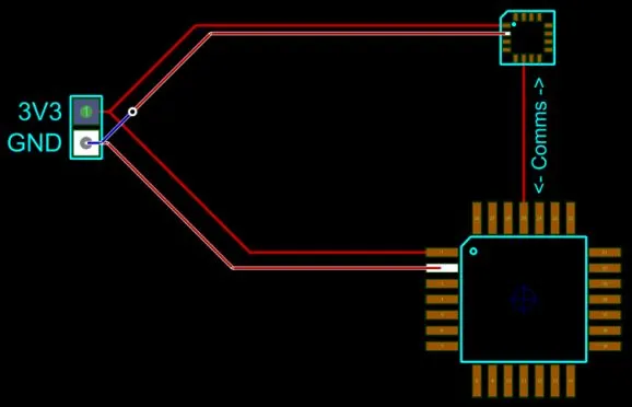
Return Current
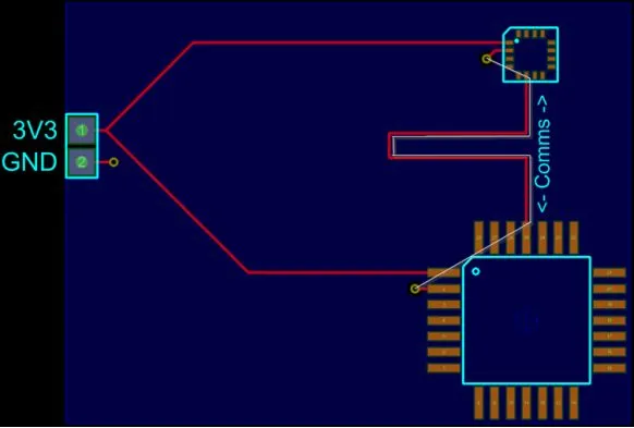
Every signal trace on a PCB requires a return path. This is usually provided by the power distribution network, for example ground (GND). Consider a board with two devices communicating, such as a microcontroller and a sensor. The signal trace between them is often the main focus, but the return current flows through the power network and may take a longer route. A longer route increases loop area and effectively creates a larger antenna. EMI/EMC design therefore must account for the return current path and keep it short to minimize radiated emissions:
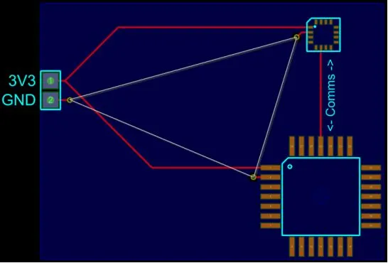
High-Speed Layout and Power Planes
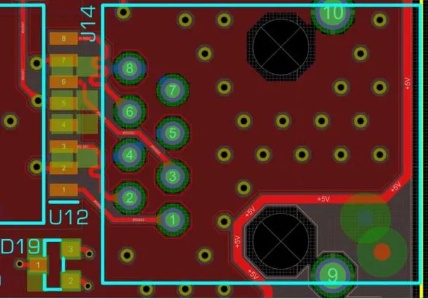
When applying high-speed design principles, boards often use internal layers as power or ground planes. Adding vias near components to connect the signal layer to the power/ground plane shortens the return path. In the diagram below, the power plane is shown in blue and the white line indicates the conceptual current path:
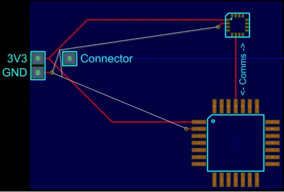
Ensure the power plane is not interrupted by splits or gaps; discontinuities force return currents to detour and increase loop area:
Maintaining a continuous plane also helps preserve constant impedance for high-speed traces, which is a core high-speed design principle:
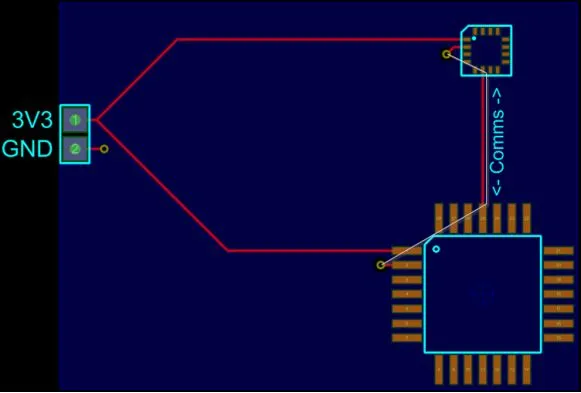
Minimum Impedance Path
DC current follows the path of least resistance, while AC current follows the path of least impedance. As frequency rises, inductive reactance becomes significant, so currents prefer paths with the lowest inductance. This causes high-frequency return current to closely follow the signal trace on the adjacent plane, which is why keeping an unbroken power or ground plane beneath high-frequency traces is important. Even if the signal meanders, its return will tend to follow directly under it at higher frequencies:
Decoupling Capacitors
When component current demands change suddenly, such as a CPU drawing more current during computation, the power traces carry transient currents and can become radiating loops. Placing adequate decoupling capacitors close to the relevant components provides a low-impedance path for AC currents between power and ground, reducing loop area and emissions:
Via Stitching
Via stitching places multiple vias to connect power or ground planes across layers. While planes may appear connected conceptually, small voltage differences can occur between layers due to changing currents and radiation. Stitching vias near ICs and along plane boundaries provides short return paths for transient currents and reduces effective antenna size:
Slew Rate
Slew rate is the speed at which a signal rises or falls. Faster edges accelerate charged particles more rapidly and generate more radiation. In the frequency domain, steeper edges contain higher-frequency components. Some microcontrollers and drivers provide configurable slew rate control to slow edges within the required signal timing, reducing high-frequency emissions. Note that slew rate must still meet the required timing; you cannot use slow edges where a high-frequency signal is required.
Staggered Switching
Devices with wide data buses may offer options to stagger switching of individual lines rather than toggling all lines simultaneously. Staggered switching spreads current transients in time, reducing the instantaneous combined EMI and helping keep emissions within acceptable levels.
Shielding
Shielding is often the first solution people consider for EMI/EMC, but it is generally a last resort after addressing layout, return path control, decoupling, and other design measures. Signals can leak through small gaps, such as the PCB edge, so shielding alone can be an ineffective patch if the root causes are not addressed. That said, shielding does have valid applications when used appropriately.
Summary
EMI/EMC design focuses on the system's AC (switching) elements and on minimizing current loop size. Designs that follow high-speed layout principles typically also perform well in EMI/EMC tests. Key practices include keeping the power plane unbroken under high-speed traces, using adequate decoupling capacitors placed close to ICs, stitching vias around switching devices and planes, and keeping high-frequency traces as short as possible. For switching converters, keep layouts small and tight with nearby decoupling. Often a noncompliant two-layer design can be fixed by moving to four layers with an internal ground plane and stitched vias near ICs. Tools such as near-field probes, TEM cells for quick pre-compliance checks, and electromagnetic scanners can help identify emission sources and verify hardware and firmware changes.