ALLPCB


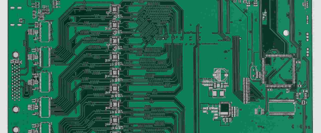
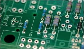
High-speed signal routing on high-layer-count PCBs demands careful attention to signal integrity, electromagnetic compatibility, and manufacturing constraints. Modern electronic systems increasingly rely on data rates exceeding several gigabits per second, which makes trace geometry, via placement, and layer stackup critical factors. Engineers must balance density requirements with the need to minimize reflections, crosstalk, and attenuation. High-layer-count boards, typically eight layers or more, provide dedicated planes for power and ground while allowing complex routing channels. This approach supports the integration of processors, memory, and high-speed interfaces in compact form factors.
Why High-Speed Routing Matters in High-Layer-Count Designs
High-layer-count PCBs enable greater component density and improved power distribution compared with simpler boards. As signal frequencies rise, the wavelength shortens, turning even short traces into transmission lines that require controlled impedance. Poor routing practices can lead to data errors, increased power consumption, and compliance failures with electromagnetic standards. High-layer boards address these issues by incorporating multiple ground planes that reduce return-path inductance and shield sensitive signals. The result is more reliable performance in applications such as networking equipment, servers, and advanced computing platforms.
Technical Principles of Signal Propagation
Signal propagation on high-layer-count PCBs follows transmission-line theory, where characteristic impedance must remain consistent along the entire path. Variations in trace width, dielectric thickness, or copper roughness alter impedance and cause reflections that degrade edge rates. Crosstalk arises when adjacent traces couple magnetically or electrically, an effect that grows stronger with faster rise times and closer spacing. Return currents flow through the nearest reference plane, so discontinuities such as via transitions or split planes force currents to take longer paths and increase radiated emissions. Dielectric losses, quantified by the dissipation factor, become significant above a few gigahertz and limit maximum trace length.
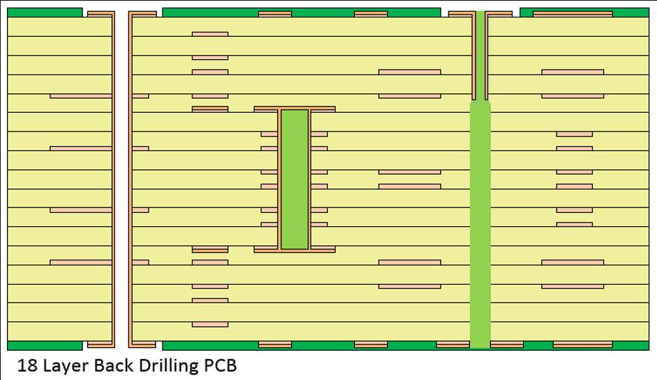
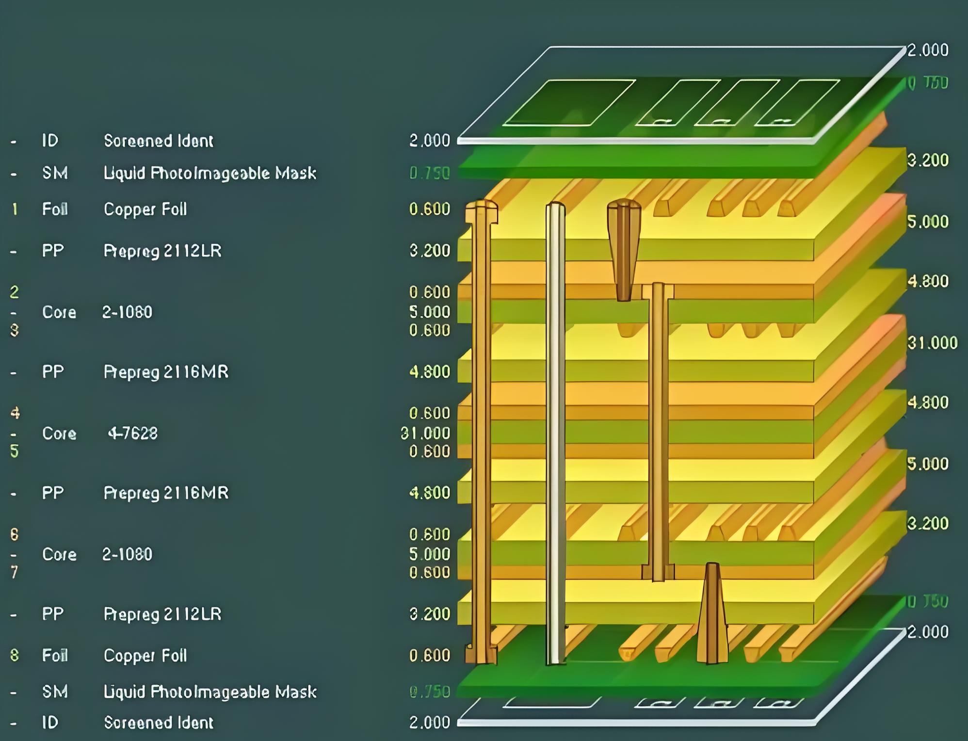
High-layer stackups typically alternate signal layers with ground or power planes to provide low-inductance return paths. This arrangement also helps control the effective dielectric constant seen by each trace. Via stubs, the unused portion of a plated through-hole, act as resonant stubs that filter high-frequency content and must be minimized through back-drilling or blind/buried via technology. Thermal expansion differences between copper and laminate materials can induce stress during reflow, affecting long-term reliability when boards undergo multiple thermal cycles.
Best Practices for Routing High-Speed Signals
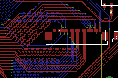
Effective high-speed routing PCB strategies begin with a well-planned layer stackup that assigns high-speed nets to inner layers adjacent to solid reference planes. Differential pairs should maintain tight coupling and equal length to preserve common-mode rejection. Trace width and spacing are calculated to achieve the target differential impedance, usually 85 or 100 ohms depending on the interface standard. Avoid 90-degree bends; instead, use 45-degree mitered corners or curved traces to reduce impedance discontinuities.
Length matching within a few mils ensures setup-and-hold timing margins at the receiver. Place decoupling capacitors close to power pins with short, wide traces or vias to minimize loop inductance. Ground vias should be located near signal vias to provide immediate return paths and reduce the area of current loops. When routing across layers, use ground stitching vias to maintain reference continuity. Simulation tools verify these choices before fabrication, allowing adjustments that keep the design within acceptable margins.
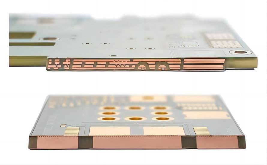
Manufacturing and Quality Considerations
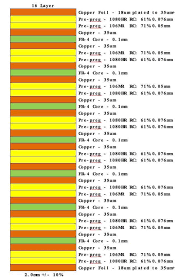
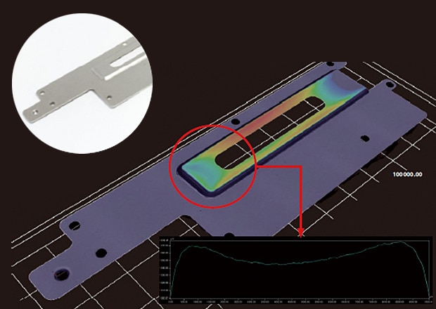
High-layer-count boards require precise control of dielectric thickness and copper plating uniformity to maintain impedance targets. IPC-6012E defines qualification and performance requirements for rigid printed boards, including conductor width and spacing tolerances that directly affect high-speed performance. During fabrication, etch factor and surface roughness influence skin-effect losses at high frequencies. Warpage control becomes more challenging with additional layers, so balanced copper distribution and symmetric stackups help keep boards flat for reliable assembly.
Conclusion
Successful high-speed routing PCB designs on high-layer-count boards combine careful stackup planning, controlled-impedance routing, and attention to return paths. These practices reduce signal degradation and improve electromagnetic compatibility. Following established design guidelines and verifying performance through simulation and testing yields boards that meet both functional and reliability requirements.
FAQs
Q1: What are the main challenges when performing high-speed routing PCB on boards with many layers?
A1: High-speed routing PCB on high-layer-count boards faces challenges such as maintaining consistent impedance, minimizing crosstalk between densely packed traces, and ensuring low-inductance return paths through multiple planes. Engineers must also manage via transitions that can introduce stubs and reflections. Thermal and mechanical stresses increase with layer count, requiring balanced stackups. Careful planning of trace geometry and reference plane placement helps address these issues while meeting timing and signal-integrity targets.
Q2: How does layer count influence PCB routing strategies for high-speed signals?
A2: Higher layer counts allow dedicated ground planes adjacent to signal layers, which improves return-path integrity and reduces electromagnetic interference. This arrangement supports tighter spacing of high-speed traces without excessive crosstalk. However, the increased number of layers demands precise control of dielectric thicknesses to achieve target impedances. Routing strategies must account for via aspect ratios and potential warpage, leading to the use of blind or buried vias in complex designs.
Q3: What techniques help control impedance during high-layer-count PCB routing?
A3: Impedance control begins with selecting appropriate trace width and dielectric thickness combinations that match the desired characteristic impedance. Reference planes must remain continuous beneath high-speed traces to provide consistent return paths. Differential pairs require matched lengths and controlled spacing to maintain the target differential impedance. Post-layout simulation confirms that manufacturing tolerances will not push impedance outside acceptable limits.
Q4: Why is via design important in high-speed signal routing on multilayer PCBs?
A4: Vias introduce inductance and potential stubs that can degrade high-frequency signals by causing reflections and resonances. Minimizing stub length through back-drilling or the use of blind vias preserves signal integrity. Placing ground vias near signal vias provides short return paths and reduces loop area. Proper via sizing and plating thickness also affect current-carrying capability and thermal performance in high-layer-count boards.
References
IPC-6012E — Qualification and Performance Specification for Rigid Printed Boards. IPC, 2017
IPC-2221B — Generic Standard on Printed Board Design. IPC, 2012
IPC-A-600K — Acceptability of Printed Boards. IPC, 2020