If you're dealing with copper plating defects or other PCB manufacturing problems, you're not alone. Copper plating is a critical step in printed circuit board (PCB) production, but issues like poor adhesion, uneven thickness, and surface roughness can lead to performance failures or costly rework. In this comprehensive guide, we'll walk you through the common challenges of copper plating, such as copper adhesion issues, plating thickness control, and copper surface roughness, and provide practical solutions to prevent these problems in your manufacturing process.
Whether you're an engineer, designer, or manufacturer, this guide will equip you with the knowledge to identify potential issues early and implement effective strategies to ensure high-quality PCB production. Let’s dive into the details of copper plating and how to tackle its challenges head-on.
What Is Copper Plating in PCB Manufacturing?
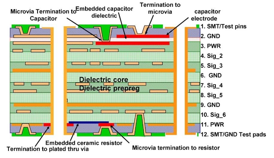
Copper plating is a vital process in PCB manufacturing where a thin layer of copper is deposited onto the board's surface and through holes (vias) to create conductive pathways. This process ensures electrical connectivity between components and layers of the PCB. Typically, copper plating is done using an electroplating method, where an electric current drives copper ions to bond with the substrate.
However, even small errors in this process can lead to significant PCB manufacturing problems. Issues like uneven plating, poor adhesion, or excessive roughness can cause signal loss, short circuits, or mechanical failures. For instance, in high-speed circuits, improper copper thickness can affect impedance, leading to signal integrity issues. Understanding the root causes of these problems is the first step toward preventing them.
Common Copper Plating Defects in PCB Manufacturing
Identifying copper plating defects early can save time and resources. Below are some of the most frequent issues encountered during PCB production, along with their causes and impacts.
1. Copper Adhesion Issues
One of the most critical copper adhesion issues occurs when the copper layer fails to bond properly to the substrate or other layers. This can result in peeling or delamination, compromising the board's reliability. Poor adhesion is often caused by surface contamination, inadequate cleaning before plating, or improper etching processes.
For example, if the substrate isn't cleaned thoroughly, oils or residues can prevent proper bonding, leading to adhesion failure under thermal stress. This is especially problematic in applications with high operating temperatures, where delamination can cause open circuits.
2. Uneven Plating Thickness
Maintaining consistent plating thickness control is essential for ensuring uniform conductivity across the PCB. Uneven thickness can lead to high-resistance areas, affecting current distribution and potentially causing overheating. This issue often arises from inconsistent current density during electroplating or poor bath chemistry management.
In high-frequency applications, uneven copper thickness can alter impedance values, disrupting signal performance. For instance, a deviation of just 0.5 mils (12.7 micrometers) in copper thickness can shift impedance by several ohms, leading to signal mismatch in a 50-ohm system.
3. Copper Surface Roughness
Excessive copper surface roughness can degrade signal integrity, especially in high-speed designs. Rough surfaces increase signal loss due to the skin effect, where high-frequency signals travel along the surface of the conductor. If the surface is too rough, it can also interfere with solderability, leading to weak connections.
Roughness is often a result of over-etching or improper plating conditions. For high-speed PCBs operating at frequencies above 1 GHz, smoother copper surfaces are critical to minimize insertion loss, which can be as high as 0.5 dB per inch in rough copper traces.
4. Blistering and Foaming
Blistering or foaming on the copper surface is a defect often linked to trapped gases or moisture during the plating process. This can weaken the copper layer and create vulnerabilities in the board. Blistering is commonly caused by poor rinse cycles, high plating temperatures, or contamination in the plating bath.
Causes of Copper Plating Issues in PCB Manufacturing
Understanding the root causes of PCB manufacturing problems related to copper plating is key to preventing them. Here are the primary factors contributing to these defects.
1. Poor Surface Preparation
Before plating, the PCB substrate must be meticulously cleaned and roughened to ensure proper adhesion. Any residue, such as fingerprints or dust, can create weak spots in the copper layer. Inadequate surface preparation is a leading cause of copper adhesion issues.
2. Improper Plating Bath Chemistry
The chemical composition of the plating bath must be carefully controlled. Imbalances in copper sulfate, sulfuric acid, or additives can lead to uneven deposition or poor quality plating. For instance, low copper ion concentration can result in thin, inconsistent layers, affecting plating thickness control.
3. Inconsistent Current Density
During electroplating, the current density across the board must be uniform. Variations can cause thicker plating in some areas and thinner in others, leading to uneven conductivity. This is particularly problematic in densely packed PCB designs with small vias.
4. Environmental Factors
Temperature, humidity, and contamination in the manufacturing environment can also impact plating quality. High humidity can introduce moisture into the process, contributing to blistering, while temperature fluctuations can affect the plating bath's performance.
Impact of Copper Plating Defects on PCB Performance
The consequences of copper plating defects can range from minor performance issues to complete board failure. Here’s how these problems affect PCB functionality:
- Signal Integrity Loss: Uneven thickness and high copper surface roughness can distort high-frequency signals, leading to data errors or communication failures in devices like routers or servers.
- Thermal Issues: Poor plating can create high-resistance spots, causing localized heating and potential damage to components.
- Mechanical Failure: Adhesion problems can lead to delamination under stress, especially in multilayer boards or during thermal cycling.
- Reduced Lifespan: Defects like blistering or cracks in the copper layer can make the PCB more susceptible to corrosion, shortening its operational life.
How to Prevent Copper Plating Issues in PCB Manufacturing
Preventing PCB manufacturing problems related to copper plating requires a combination of best practices, process control, and quality assurance. Below are actionable strategies to ensure high-quality plating results.
1. Optimize Surface Preparation
Ensure thorough cleaning and micro-etching of the substrate before plating. Use chemical cleaners to remove organic residues and oxides, and maintain a consistent surface texture to promote adhesion. Regularly inspect cleaning equipment to avoid contamination.
2. Monitor Plating Bath Chemistry
Regularly test and adjust the plating bath composition to maintain optimal levels of copper ions, acids, and additives. Automated systems can help monitor pH and temperature, ensuring stability during the plating process. For example, maintaining a copper sulfate concentration of 75-100 g/L can help achieve uniform deposition.
3. Control Current Density
Use advanced plating equipment with precise current control to ensure even distribution across the board. For complex designs, consider using pulse plating techniques to improve uniformity in high-density areas and small vias.
4. Minimize Copper Surface Roughness
For high-speed applications, select plating processes and additives that produce smoother copper deposits. Post-plating treatments, such as chemical polishing, can also reduce surface roughness to below 0.5 micrometers, improving signal performance at frequencies above 1 GHz.
5. Implement Strict Quality Control
Conduct regular inspections using tools like X-ray fluorescence (XRF) to measure copper thickness and ensure it meets specifications (typically 1-2 oz/ft2 or 35-70 micrometers for standard boards). Use microsection analysis to check for adhesion and internal defects in multilayer PCBs.
Advanced Techniques for Copper Plating in PCB Manufacturing
For manufacturers looking to push the boundaries of quality, advanced techniques can further enhance copper plating results and address persistent challenges.
1. Reverse Pulse Plating
This method alternates between forward and reverse current during plating, improving uniformity and reducing defects in high-aspect-ratio vias. It’s particularly effective for achieving consistent plating thickness control in complex designs.
2. Copper Wrap Plating for Vias
In multilayer boards, copper wrap plating ensures continuous plating from the via hole to the surface foil, enhancing reliability. This technique is critical for high-density interconnect (HDI) boards where via failures can be catastrophic.
3. Use of Low-Roughness Copper Foils
Starting with low-roughness copper foils can minimize copper surface roughness from the outset. These foils are designed for high-frequency applications and can reduce signal loss by up to 20% compared to standard foils.
Conclusion: Building Reliable PCBs with Flawless Copper Plating
Copper plating is at the heart of PCB manufacturing, but it comes with challenges that can lead to costly PCB manufacturing problems. By understanding common copper plating defects like copper adhesion issues, uneven plating thickness control, and excessive copper surface roughness, you can take proactive steps to prevent these issues. From optimizing surface preparation to leveraging advanced plating techniques, the strategies outlined in this guide will help you achieve consistent, high-quality results.
At ALLPCB, we’re committed to supporting engineers and manufacturers in overcoming these challenges with cutting-edge solutions and expertise. By implementing strict quality control and staying updated on best practices, you can ensure your PCBs meet the highest standards of performance and reliability, no matter the application.
 ALLPCB


