 ALLPCB


Introduction
In high-frequency PCB design, vias serve as critical interconnects between layers, but their configuration directly influences signal integrity. As signal speeds increase beyond gigabit rates, even minor imperfections in via geometry can lead to degradation through reflections, crosstalk, and attenuation. High-frequency PCB via design requires careful consideration of parasitic effects to maintain waveform fidelity and minimize bit error rates. Engineers must balance electrical performance with manufacturability, ensuring vias support data rates in the tens of gigabits per second. This article explores the mechanisms behind via-related signal issues and practical strategies for optimization. Understanding these principles enables designers to achieve robust performance in applications like telecommunications and computing.
Understanding Vias and Their Role in High-Frequency PCBs
Vias are plated through-holes that provide vertical electrical connections in multilayer boards. In high-frequency environments, through-hole vias dominate due to cost and reliability, yet they introduce discontinuities in the transmission path. Blind and buried vias offer alternatives by limiting the connection span, reducing unwanted extensions or stubs. Via stubs occur when the plated barrel extends beyond the signal path, acting as a resonant element that reflects energy back toward the source. These effects become pronounced above 1 GHz, where wavelengths approach board dimensions. Proper high-frequency PCB via design mitigates these issues by aligning via structure with signal requirements.
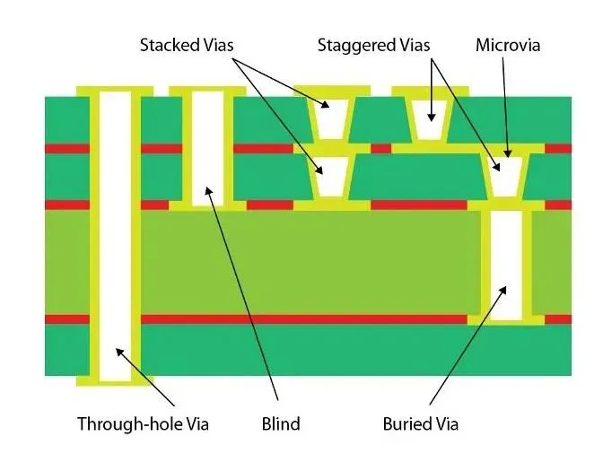
Signal integrity via optimization starts with selecting the appropriate via type based on layer count and frequency. Through vias suit simpler boards but falter in dense, high-speed layouts due to longer stubs. Blind vias connect surface to inner layers, while buried vias link inner layers exclusively, both minimizing exposure to electromagnetic interference. Fabricators adhere to standards like IPC-2221 for generic design guidelines on via dimensions and spacing. This structured approach ensures vias contribute positively to overall board performance rather than becoming bottlenecks.
The Mechanisms of Via-Induced Signal Degradation
Via inductance arises primarily from the loop area formed by the current path through the barrel and return plane. In high frequencies, this self-inductance causes voltage drops and delays, distorting rising edges. Capacitance between the via barrel and surrounding planes further complicates impedance matching, leading to ringing. The combination amplifies at transitions, where characteristic impedance mismatches generate reflections. Engineers model these parasitics using field solvers to predict behavior before fabrication. Minimizing via inductance requires geometric tweaks that reduce effective length and increase diameter.
Via stub effects represent a dominant concern in multilayer boards. Unused stub lengths resonate at quarter-wavelength frequencies, creating periodic nulls in insertion loss. For instance, a stub equal to one-quarter wavelength at the operating frequency acts as a short circuit, severely attenuating the signal. These resonances shift with frequency, complicating broadband performance. Simulations reveal that stubs longer than a fraction of the wavelength degrade eye diagrams by introducing jitter and closure. Addressing via stub effects through targeted techniques restores signal margins.
Crosstalk between adjacent vias compounds these issues in dense routing. Mutual inductance couples signals, injecting noise from aggressor to victim lines. Ground vias nearby provide return paths, shielding sensitive nets. Discontinuities at via transitions also radiate energy, coupling to nearby traces. Comprehensive analysis considers both near-end and far-end crosstalk. High-frequency PCB via design thus demands holistic optimization of spacing and shielding.
Via Stub Effects and Their Quantification
Via stubs primarily cause return loss through impedance discontinuities. The stub presents a reactive load that reflects incident waves, with reflection coefficient depending on stub length relative to wavelength. Shorter stubs shift resonances higher, but complete elimination proves ideal for wideband signals. In practice, stub lengths correlate with board thickness and layer pairing. Designers target stub removal where signals traverse fewer layers. This principle underpins strategies like selective via usage.
Empirical studies confirm stub dominance in signal degradation. Resonance frequencies scale inversely with stub length, with antipad size playing a minor role. Test methods outlined in IPC-TM-650 quantify these effects via de-embedding techniques. Minimizing via stub lengths below critical thresholds preserves flat frequency response. Engineers prioritize signals with tight timing budgets for stub mitigation. Such data-driven decisions enhance reliability across operating bands.
Practical Solutions: Backdrilling and Beyond
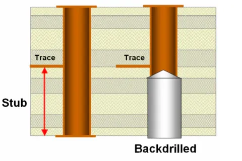
Back drilling PCB techniques remove excess stub material post-plating, creating a clearance hole that terminates the via at the active layer. This process employs larger diameter drills to avoid damaging inner connections, typically leaving a 0.15 mm shoulder. Backdrilling suits thick boards where blind vias prove uneconomical. It reduces effective stub to near zero, eliminating major resonances. Fabricators control depth precisely using pilot holes and optical verification. This method proves essential for signals exceeding multi-gigabit speeds.
Minimizing via inductance involves multiple tactics. Larger via diameters lower inductance per unit length, while arrays of vias parallel paths for high currents. Ground via fences around signal vias confine return currents, reducing loop area. Via-in-pad configurations embed pads directly, smoothing transitions. Staggered antipads prevent coupling. These combined measures optimize impedance profiles.
Signal integrity via optimization extends to stackup planning. Pairing signal layers with adjacent planes stabilizes reference for return paths. Controlled depth routing aligns vias with nets. Post-layout verification confirms margins via time-domain reflectometry. Adherence to IPC-6012F performance specs ensures qualification. Iterative refinement bridges simulation and reality.
- Backdrilling — Stub elimination — Thick multilayer boards
- Blind/Buried Vias — Reduced length — HDI designs
- Via Arrays — Lower inductance — Power delivery networks
- Ground Via Shielding — Crosstalk reduction — Dense high-speed routing
Advanced Best Practices for High-Frequency Designs
Layer sequencing minimizes via count by localizing signals. Direct layer-to-layer transitions via microvias suit ultra-high densities. Elliptical vias align with trace orientation, preserving field uniformity. Solder-filled vias enhance thermal relief without parasitics. Prepreg selection influences dielectric uniformity around barrels. These refinements compound benefits.
Fabrication tolerances impact via quality. Plating uniformity prevents barrel cracks under thermal stress. Aspect ratios below 10:1 ensure void-free fills. Inspection verifies stub depths post-backdrill. Collaboration with manufacturers refines rulesets. Sustained performance demands these details.
Conclusion
Via design profoundly shapes signal integrity in high-frequency PCBs, with stubs, inductance, and discontinuities as chief adversaries. Techniques like backdrilling, blind vias, and shielding provide proven countermeasures. Logical application of these principles, guided by standards, yields robust designs. Engineers achieve optimization by integrating simulation, stackup strategy, and fabrication awareness. Prioritizing high-frequency PCB via design ensures future-proof performance amid rising speeds. Mastering these elements elevates board reliability and efficiency.
FAQs
Q1: What are via stub effects in high-frequency PCB via design?
A1: Via stub effects arise when unused portions of through-hole vias resonate, causing signal reflections and insertion loss peaks at quarter-wavelength frequencies. These degrade eye diagrams and increase jitter in multi-gigabit links. Mitigation involves shortening stubs or removing them; backdrilling effectively eliminates stubs for critical nets, and logical stackup planning prevents excessive lengths upfront.
Q2: How does back drilling PCB improve signal integrity?
A2: Back drilling PCB removes via stubs by counter-boring excess barrel, reducing resonances and reflections in high-speed paths while preserving inner connections. It minimizes effective inductance and is ideal for thick boards. Careful depth control creates clean shoulders without damage, aligning performance with modern multi-gigabit protocols.
Q3: What strategies minimize via inductance for signal integrity via optimization?
A3: Reduce via inductance by using larger diameters, shorter lengths, and parallel via arrays to shrink loop area. Add ground via clusters for low-impedance return paths, use via-in-pad with appropriate fills to smooth transitions, and tune antipad sizing via simulation. These measures help maintain impedance continuity across frequencies.
Q4: Why is high-frequency PCB via design critical for electrical engineers?
A4: High-frequency PCB via design controls parasitics that can degrade signal quality, ensuring clean waveforms and reliable links. By addressing stubs, crosstalk, and impedance mismatches—and applying standards like IPC-2221—engineers sustain data integrity at rising speeds, reduce risk of respins, and deliver robust, future-proof designs.
References
IPC-2221B — Generic Standard on Printed Board Design. IPC, 2003
IPC-6012F — Qualification and Performance Specification for Rigid Printed Boards. IPC, 2023
IPC-TM-650 — Test Methods Manual. IPC, current


