ALLPCB


Surveillance systems depend on image sensors mounted directly onto printed circuit boards to capture and process visual data. The selection of an image sensor influences overall system performance, power consumption, and signal integrity within the PCB assembly. Engineers must evaluate sensor technologies alongside PCB layout constraints to achieve reliable operation across diverse lighting conditions. Integration considerations include data transmission rates, thermal dissipation, and electromagnetic compatibility. These factors determine how effectively the completed board supports continuous monitoring applications.
Why Image Sensor Selection Matters for Surveillance PCBs
Image sensor choice directly affects the ability of a surveillance PCB to deliver clear footage in varying environments. Low-light image sensor PCB designs require sensors that maintain sensitivity without excessive noise amplification. High-resolution camera PCB configurations demand robust interfaces to handle increased data volumes while preserving signal quality. PCB for night vision cameras often incorporates sensors optimized for extended wavelength response. Proper matching of sensor characteristics to board architecture supports consistent performance and reduces the need for post-processing corrections.
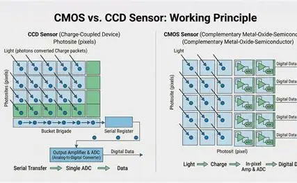
CMOS versus CCD Technologies for Surveillance Applications
CMOS and CCD image sensors differ in their internal architectures and resulting electrical behaviors on a PCB. CMOS sensors integrate analog-to-digital conversion and timing circuitry on the same die, which simplifies routing on the supporting board and lowers overall power draw. CCD sensors transfer charge across the array before conversion, typically requiring additional external circuitry that increases board complexity and trace length. In surveillance settings, CMOS devices generally provide faster readout speeds suitable for real-time processing. CCD devices have historically offered advantages in uniform charge transfer that can reduce certain fixed-pattern artifacts. Modern CMOS implementations incorporate backside illumination and stacked architectures that narrow performance gaps in low-light scenarios.
Key PCB Design Considerations for Image Sensor Integration
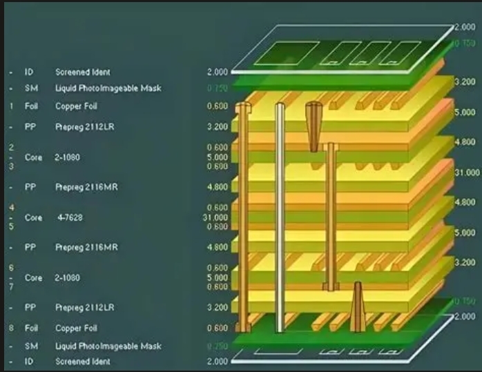
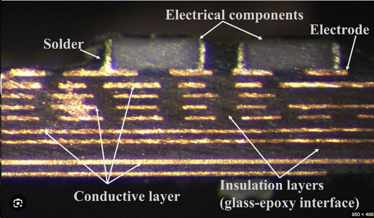
Placing an image sensor on a surveillance PCB requires attention to high-speed differential pairs that carry pixel data to the processor. Controlled impedance routing minimizes reflections and maintains signal integrity at multi-megapixel resolutions. Power delivery networks must supply clean voltage rails to the sensor while decoupling high-frequency noise from digital sections. Thermal vias and copper pours help dissipate heat generated by continuous operation, particularly in enclosed camera housings. Ground plane partitioning reduces crosstalk between analog sensor outputs and digital control lines. Component placement follows sequential signal flow to shorten critical paths and limit electromagnetic interference.
Best Practices for Low-Light and Night-Vision PCB Configurations
Engineers optimize low-light image sensor PCB performance by selecting sensors with high quantum efficiency and low dark current characteristics. PCB for night vision cameras benefits from layouts that support supplemental infrared illumination sources without introducing additional noise. Careful selection of lens mount alignment features on the board ensures optical axis stability relative to the sensor die. Filtering and shielding techniques around the sensor area protect against ambient electromagnetic fields common in outdoor installations. Assembly processes must maintain precise coplanarity between the sensor package and board surface to avoid focal plane tilt. These practices collectively improve image quality while respecting the mechanical and electrical constraints of the finished assembly.

Assembly and Reliability Considerations
Surface-mount attachment of image sensors follows established procedures that protect sensitive optical windows during reflow. Moisture sensitivity levels of the sensor package dictate baking requirements prior to soldering to prevent delamination. Post-assembly inspection verifies both electrical connectivity and mechanical alignment critical for optical performance. Environmental testing confirms that the completed surveillance PCB maintains functionality across temperature and humidity ranges typical of deployed systems. These steps support long-term reliability without introducing defects that could degrade image quality over time.
Conclusion
Selecting an image sensor for a surveillance PCB involves balancing optical performance requirements with electrical and mechanical constraints of the board. CMOS technology offers integration advantages that simplify many designs, while CCD options remain relevant where specific uniformity characteristics are needed. Attention to layout, power integrity, and thermal management ensures the final assembly meets operational demands in low-light and night-vision scenarios. Following structured design practices leads to reliable, high-performing surveillance solutions.
FAQs
Q1: What factors influence CMOS versus CCD selection for a surveillance PCB?
A1: Engineers evaluate power consumption, readout speed, and integration complexity when comparing the two technologies. CMOS sensors typically reduce board-level component count and support higher frame rates, which benefits real-time surveillance. CCD sensors may require additional support circuitry that increases trace routing demands. The final decision also considers low-light sensitivity needs and overall system power budget.
Q2: How does a low-light image sensor PCB differ from standard designs?
A2: Low-light image sensor PCB layouts emphasize clean power delivery and minimal noise coupling to preserve weak signals from the sensor. Extended exposure times and higher analog gain settings increase susceptibility to interference, requiring tighter control of return paths and shielding. Thermal management becomes more critical because continuous operation at elevated gain levels generates additional heat on the board.
Q3: What PCB features support high-resolution camera PCB performance?
A3: High-resolution camera PCB designs incorporate wide data buses or high-speed serial interfaces capable of handling increased pixel throughput. Controlled-impedance differential pairs and adequate ground planes maintain signal integrity across longer board distances. Adequate decoupling capacitance near the sensor prevents voltage droop during burst readouts that could introduce artifacts.
Q4: Why is thermal management important in a PCB for night vision cameras?
A4: Night-vision applications often operate in sealed enclosures where heat buildup can raise sensor temperature and increase dark current noise. Copper pours, thermal vias, and strategic component spacing help conduct heat away from the image sensor die. Maintaining lower operating temperatures preserves image quality during extended low-light monitoring periods.
References
IPC-6012E — Qualification and Performance Specification for Rigid Printed Boards. IPC, 2017
JEDEC J-STD-020E — Moisture/Reflow Sensitivity Classification. JEDEC, 2014
IPC-A-600K — Acceptability of Printed Boards. IPC, 2020