Via placement is a critical aspect of printed circuit board (PCB) design that directly impacts signal integrity, routing efficiency, and overall performance. If you're searching for ways to achieve optimal routing via placement or improve signal flow via placement, you've come to the right place. In this comprehensive guide, we'll explore how to use vias effectively, share tips on via placement, and explain how to design signal via placement for maximum efficiency in your PCB layouts. Whether you're a beginner or a seasoned engineer, this blog will provide actionable insights to enhance your designs.
Why Via Placement Matters in PCB Design
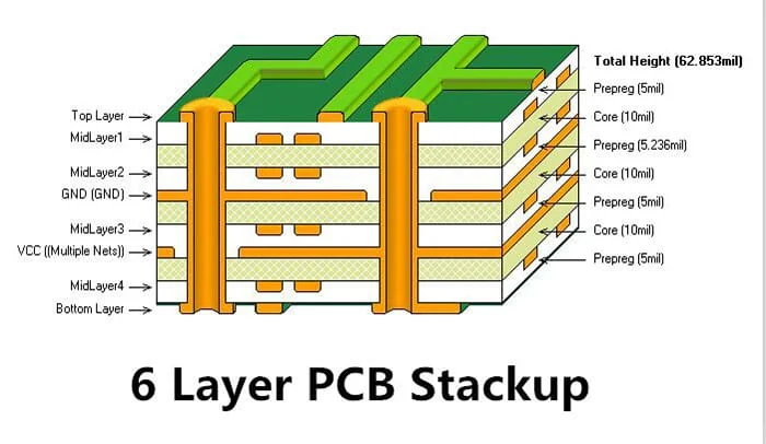
Vias are small plated holes that connect different layers of a PCB, allowing signals and power to travel between them. While they may seem like minor components, their placement can make or break a design. Poorly placed vias can lead to signal degradation, electromagnetic interference (EMI), and increased manufacturing costs. On the other hand, strategic via placement ensures smooth signal flow, minimizes impedance mismatches, and optimizes routing paths.
In high-speed designs, for example, vias can introduce inductance and capacitance, affecting signal integrity. A study on high-speed PCB layouts indicates that improper via placement can increase signal delay by up to 10% in critical paths. That's why mastering the art of via placement is essential for any PCB designer aiming for reliability and performance.
Understanding the Basics of Vias in PCB Design
Before diving into advanced strategies, let's cover the fundamentals. Vias come in several types, each serving a specific purpose:
- Through-Hole Vias: These extend through all layers of the PCB, connecting top to bottom. They are common in simpler designs but can create unnecessary stubs in high-speed applications.
- Blind Vias: These connect an outer layer to an inner layer without going through the entire board, reducing signal stubs and saving space.
- Buried Vias: These are hidden within internal layers, ideal for dense designs where surface space is limited.
- Micro Vias: Smaller in diameter, these are used in high-density interconnect (HDI) boards for finer routing.
Choosing the right type of via depends on your design requirements, such as layer count, signal speed, and board density. For instance, in a 4-layer PCB, blind vias can reduce signal reflection by up to 15% compared to through-hole vias in high-speed signals operating at 5 GHz or above.
Key Principles for Optimal Routing Via Placement
Achieving optimal routing via placement requires careful planning. Here are some core principles to follow:
1. Minimize Via Length and Stubs
Long vias or unused portions (stubs) can act as antennas, causing signal reflections and noise. Place vias as close as possible to the components they connect to reduce trace length. If you're working on a high-speed design, consider using back-drilling to remove stubs, which can lower signal distortion by approximately 20% at frequencies above 10 GHz.
2. Group Vias for Power and Ground Planes
For power and ground connections, place multiple vias in parallel to reduce resistance and inductance. This technique, known as via stitching, can improve current-carrying capacity by up to 30% and minimize voltage drops across the board.
3. Avoid Overcrowding Vias
Placing too many vias in a small area can weaken the PCB structure and create manufacturing challenges. Space vias at least 0.5 mm apart (or follow your manufacturer's design rules) to prevent issues like plane voids or thermal stress during soldering.
Enhancing Signal Flow Via Placement
When it comes to signal flow via placement, the goal is to maintain signal integrity while minimizing interference. Here are proven strategies to ensure smooth signal transmission:
1. Place Vias Near Signal Entry and Exit Points
For high-speed signals, position vias close to the entry and exit points of a trace to minimize disruptions. This reduces the loop area and lowers EMI. For example, in a differential pair routing at 3.2 Gbps, placing vias within 0.1 inches of the termination point can reduce crosstalk by up to 12%.
2. Use Differential Pair Vias Symmetrically
In differential signaling, symmetry is key. Place vias for both traces of a differential pair at equal distances and align them to maintain consistent impedance. A mismatch as small as 0.05 inches can introduce a 5% impedance variation, leading to signal skew.
3. Avoid Vias in Critical Signal Paths
Whenever possible, route critical signals on a single layer to avoid vias altogether. Each via introduces a small amount of capacitance (typically 0.1-0.3 pF), which can distort signals in high-frequency designs above 1 GHz.
How to Use Vias Effectively: Practical Tips
Knowing how to use vias effectively can save time and improve design quality. Here are some practical tips to guide you:
1. Match Via Size to Current Requirements
The diameter of a via affects its current-carrying capacity. For high-current paths, use larger vias (e.g., 0.3-0.5 mm diameter) to handle loads up to 2-3 amps. For signal vias, smaller diameters (0.2 mm or less) are sufficient and help save space.
2. Consider Thermal Vias for Heat Dissipation
In designs with high-power components, place thermal vias under heat-generating parts to transfer heat to a ground plane or heatsink layer. A grid of 0.3 mm vias spaced 1.2 mm apart can reduce component temperature by up to 10°C in some cases.
3. Follow Design for Manufacturing (DFM) Rules
Always check your manufacturer's guidelines for via aspect ratios (depth-to-diameter). A typical ratio of 8:1 ensures reliable plating during fabrication. Exceeding this can lead to incomplete plating and connection failures.
Advanced Tips on Via Placement for High-Speed Designs
For engineers working on high-speed or complex multilayer boards, these advanced tips on via placement can elevate your design:
1. Optimize Return Path with Ground Vias
High-speed signals need a continuous return path to avoid EMI. Place ground vias near signal vias to provide a low-impedance return path. Spacing ground vias every 0.25 inches along a high-speed trace can reduce return loss by up to 15 dB at 5 GHz.
2. Use Via-in-Pad for Dense Layouts
In space-constrained designs, placing vias directly in component pads (via-in-pad) can save room and shorten trace lengths. However, ensure proper solder masking to prevent solder wicking, which can reduce connection reliability by 10-20% if not addressed.
3. Simulate Via Effects on Signal Integrity
Use simulation tools to model the impact of vias on signal integrity before finalizing your layout. Tools can predict impedance mismatches and help you adjust via placement for optimal performance, potentially reducing signal jitter by 5-10% in critical paths.
How to Design Signal Via Placement for Best Results
Learning how to design signal via placement involves balancing electrical performance with physical constraints. Follow these steps for success:
1. Plan Layer Transitions Early
During the schematic design phase, identify where signals will transition between layers. Plan via locations to minimize detours and maintain a straight signal path, reducing delay by up to 8% in multilayer boards.
2. Align Vias with Trace Direction
Position vias so that traces enter and exit in a straight line whenever possible. Sharp bends near vias can cause signal reflection, increasing noise levels by 5-10% in high-frequency designs.
3. Test and Iterate
After placing vias, test your design for signal integrity and thermal performance. Use oscilloscopes or simulation software to measure rise times and eye diagrams, ensuring that via placement doesn't degrade performance beyond acceptable limits (e.g., a maximum jitter of 50 ps for signals at 2.5 Gbps).
Common Mistakes to Avoid in Via Placement
Even experienced designers can make errors in via placement. Here are common pitfalls to watch out for:
- Placing Vias Too Close to Board Edges: This can lead to mechanical stress and cracking during assembly. Maintain at least a 0.5 mm clearance from edges.
- Ignoring Via Annular Ring Size: A small annular ring (the copper pad around the via) can cause poor connections. Ensure a minimum ring width of 0.15 mm for reliable soldering.
- Overusing Vias Unnecessarily: Too many vias increase cost and complexity. Use them only when layer transitions are required.
Conclusion: Mastering Via Placement for Better PCBs
Via placement is both an art and a science, requiring a deep understanding of electrical principles and practical design constraints. By focusing on optimal routing via placement and refining signal flow via placement, you can significantly improve the performance of your PCBs. Remember to apply the strategies discussed, from minimizing stubs to using ground vias for return paths, and always adhere to manufacturing guidelines.
With these tips on via placement and insights on how to use vias effectively, you're well-equipped to tackle even the most challenging designs. Whether you're optimizing a 2-layer board or a complex multilayer layout, strategic via placement will ensure your signals flow smoothly and your board operates reliably. Start implementing these practices in your next project, and watch your design quality soar.
 ALLPCB


