ALLPCB


Overview
CPU and DRAM are the two core components in servers. Memory interface ICs are integrated into DRAM modules and serve as the core logic devices for server memory modules. Their primary role is to improve data access speed and stability to meet the growing performance and capacity requirements of server CPUs. Because CPUs process data faster than memory, interface ICs are added to meet requirements for operating speed, signal integrity, and stability.
DRAM and DDR evolution
DRAM, with its simple structure and compact design, has dominated server memory and evolved from DRAM to SDRAM and then to the DDR SDRAM family. SDRAM is synchronous dynamic random access memory, meaning its operation is referenced to a clock and it transfers data on the clock rising edge. DDR SDRAM, or double data rate SDRAM, transfers data on both rising and falling clock edges, yielding twice the data rate of SDRAM per clock cycle. To increase transfer rates and reduce power consumption, the DDR standard has evolved through DDR1 to DDR5.
Server CPUs and DDR5 adoption
New generations of server CPUs can stimulate system upgrades. Intel and AMD, as major server CPU vendors, have released advanced server processors supporting DDR5. For example, Intel's latest Xeon processors and AMD's fourth-generation EPYC processors support 8-channel and 12-channel DDR5 configurations respectively.
Historically, a new DDR generation reaches roughly 20-30% adoption in the first year after initial volume, 50-70% by the end of the second year, and majority penetration by the third year. Although DDR5 adoption lagged expectations in 2022, it is expected to accelerate, with server deployments below 20% in 2023 and rising toward about 70% by 2025.
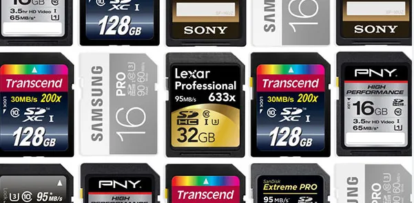
Memory interface IC types
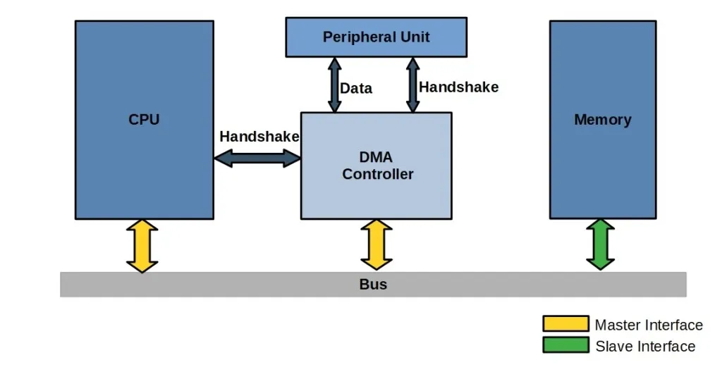
Memory interface ICs are functionally divided into two categories. Registered clock drivers (RCD) buffer address/command/control signals from the memory controller. Data buffers (DB) buffer data signals from the memory controller or DRAM devices. Modules that only use RCD chips to buffer address/command/control signals are typically called RDIMM, while modules that use both RCD and DB chips to buffer address/command/control and data signals are called LRDIMM.
Market drivers and module changes
1) Server demand recovery and higher CPU counts per chassis. After a slump from 2019 to 2021, global server shipments rebounded in 2022. Server types include AI servers and general-purpose servers. AI servers started later but grew rapidly; AI server shipments were about 1% of the total in 2022 and are forecast to grow at a high CAGR from 2023 to 2025. General-purpose servers are expected to grow steadily at a moderate CAGR.
Large AI models have increased compute requirements, driving higher CPU counts per server. Recent systems from major vendors cite standard and maximum CPU configurations of 4 to 8 processors per system, a marked increase compared with servers several years earlier.
2) Replacement cycle driven by DDR5 upgrades. Since the DDR5 standard was finalized in 2020, server vendors have planned DDR5-compatible platforms. In the DDR4 generation, a typical LRDIMM might include 1 RCD and 9 DB chips. Under DDR5, an LRDIMM will typically use 1 RCD and 10 DB devices and will also require supporting devices such as an SPD serial EEPROM, a power management IC (PMIC), and one to three temperature sensors. DDR5 modules introduce PMICs for improved power management, creating incremental demand for DB chips and module companion ICs.
3) Faster DDR5 sub-generation cycles and stable average selling prices. Within a given product generation, unit prices generally decline year over year, but each new sub-generation typically launches at a higher price than its predecessor. Shorter iteration cycles for DDR5 sub-generations can help maintain a stable ASP for memory interface ICs.
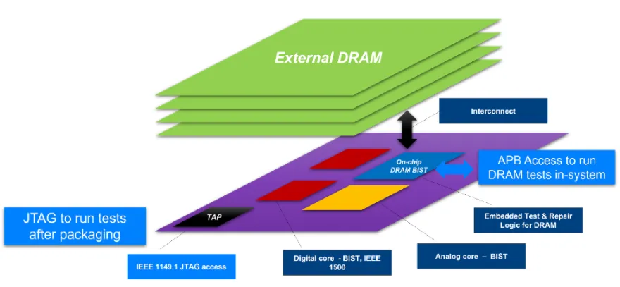
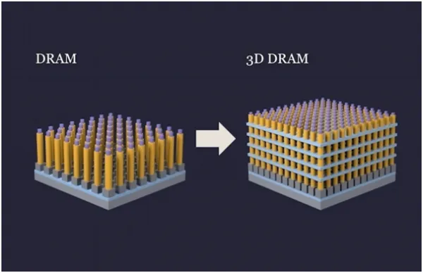
High Bandwidth Memory (HBM)
High Bandwidth Memory, initiated by AMD and SK Hynix, is a high-performance DRAM based on 3D stacking technology, suitable for applications requiring very high memory bandwidth such as GPUs and high-performance networking equipment. Under the HBM2E specification, at 3.6 Gbps per pin an HBM2E stack can deliver around 461 GB/s of memory bandwidth per stack. HBM2E supports up to 12 DRAM die stacks and capacities up to 24 GB per stack.
HBM stacks are vertically integrated and connected to the CPU or GPU via an interposer, minimizing data transfer distances. This design yields advantages in power, performance, and footprint compared with discrete DRAM solutions.
CXL and PCIe interconnects
Compute Express Link, or CXL, provides high compatibility and memory coherency, enabling it to rapidly supplant legacy PCIe usage in data center environments as a leading interconnect standard. CXL is designed to be compatible at the physical interface level with PCIe 5.0, allowing many existing processors, GPUs, and FPGAs that support PCIe ports to adopt CXL. CXL addresses PCIe limitations in memory efficiency, latency, and throughput and is being promoted as an optional protocol operating above the PCIe physical layer.
CXL enables coherent, low-latency interconnects between CPUs and accelerators such as GPUs and FPGAs, maintaining memory coherence between CPU address space and device memory. That allows CPU and GPU to share memory resources with lower latency, effectively forming a large pooled memory space across devices and reducing data movement costs.
With backing from major CPU vendors including AMD, ARM, IBM, and Intel, CXL has become a leading industry standard. Estimates suggest meaningful market potential for CXL-related products driven by heterogeneous computing growth.
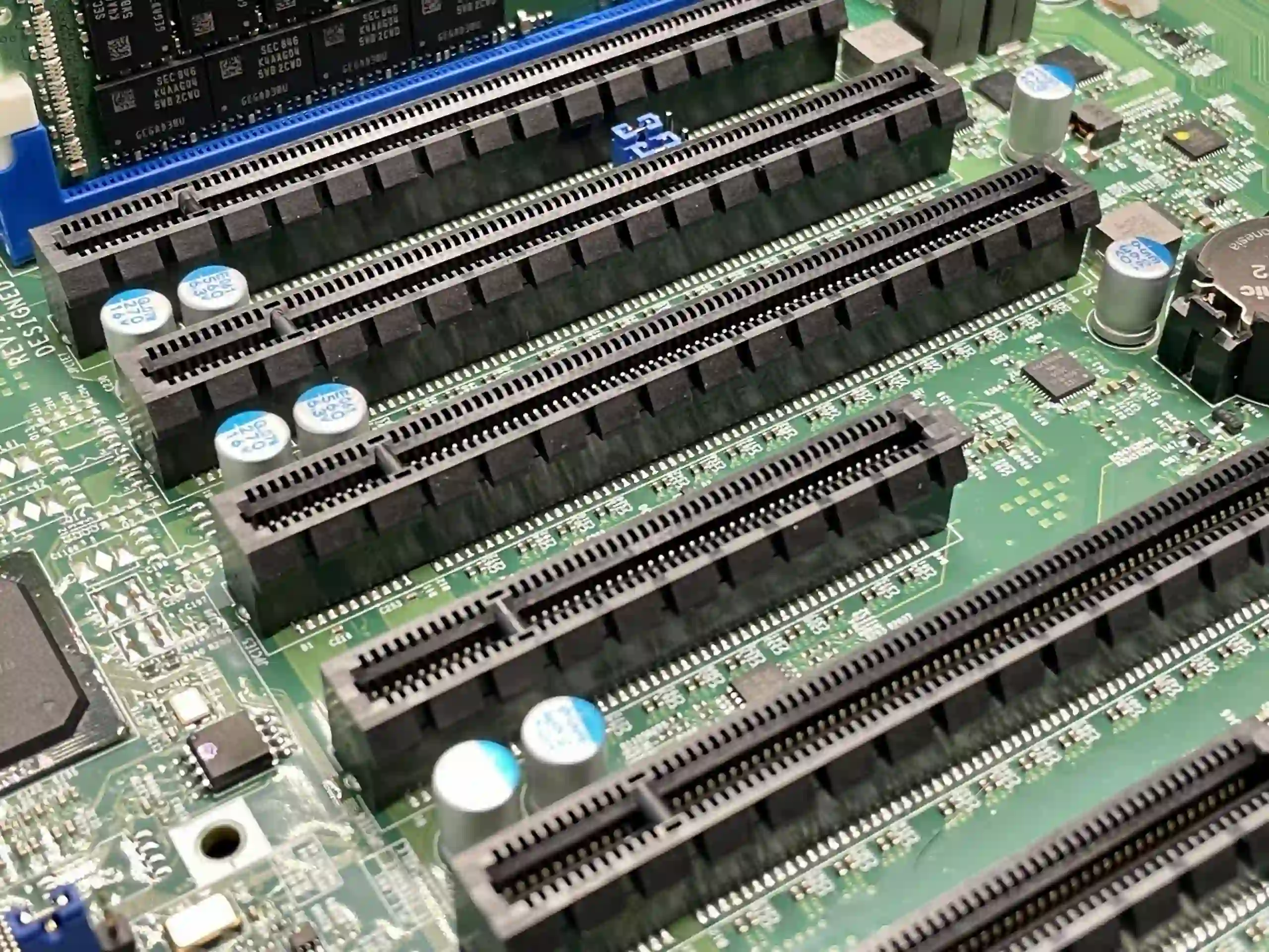
PCIe trends and signal integrity
PCIe remains the most widely used high-speed bus, offering high transfer rates, broad compatibility, and expandability. As system data rates increase, the industry has shifted from parallel buses to high-speed serial links. PCIe has evolved from legacy PCI, AGP, and PCI-X, and its per-lane transfer rate has nearly doubled with each generation. For example, PCIe 4.0 operates at 16 GT/s per lane and PCIe 5.0 at 32 GT/s per lane. At the same time, the link insertion loss budget has tightened, increasing from about 28 dB in the PCIe 4.0 era to about 36 dB in the PCIe 5.0 era. Signal attenuation and loss of signal integrity are key challenges limiting the application of next-generation high-speed protocols.