ALLPCB


Overview
As circuit board designs and component packages shrink and OEMs demand higher-speed systems, electromagnetic compatibility (EMC) and related electromagnetic interference (EMI) have become major challenges for PCB layout and design engineers.
EMC is closely related to the generation, propagation, and reception of electromagnetic energy, and PCB designs aim to avoid EMC issues. Electromagnetic energy comes from multiple sources and mixes together, so designers must take care to ensure that different circuits, traces, vias, and PCB materials work together so signals remain compatible and do not interfere.
Grounding
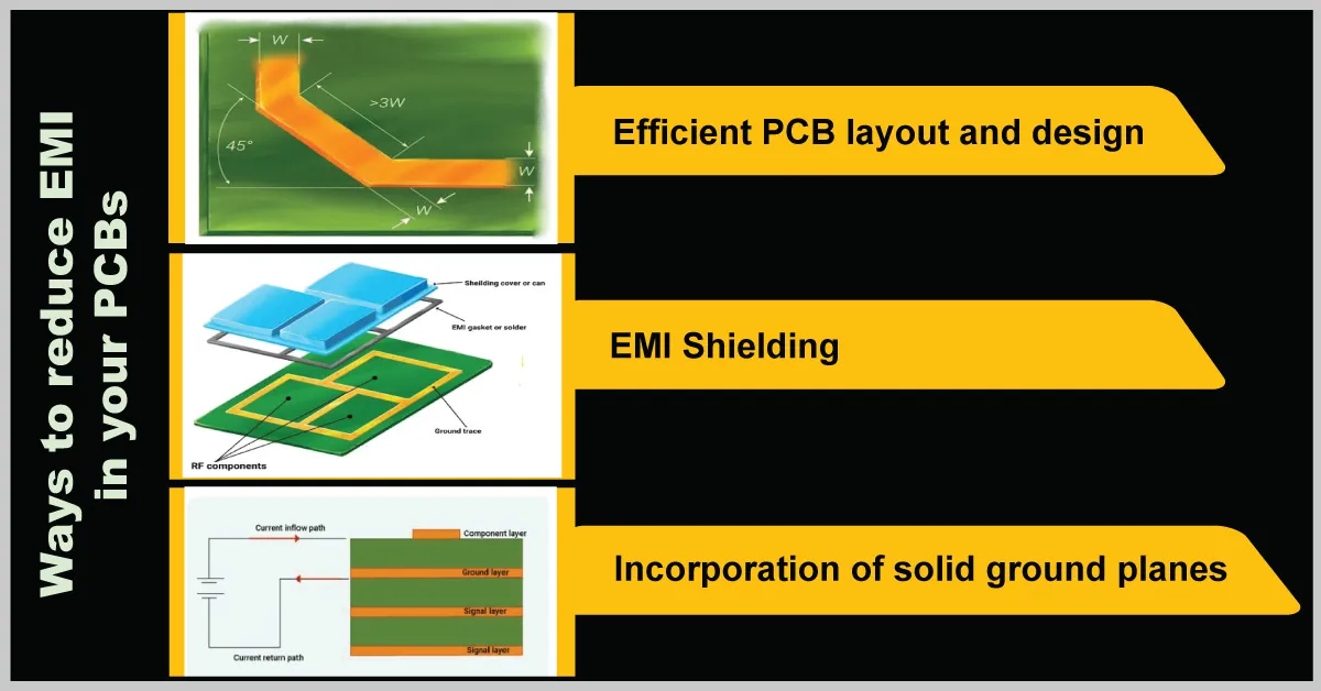
One key method to reduce EMI is careful PCB ground plane design. The first step is to maximize ground area across the PCB, which helps reduce emissions, crosstalk, and noise. Special care is required when connecting each component to a ground point or ground plane; without proper connections, the neutralizing effect of a solid ground plane cannot be fully realized.
The length and integrity of the signal return path are also critical. The round-trip timing between a signal and its return must be consistent; otherwise antenna-like behavior can occur and radiated energy contributes to EMI. Traces carrying current to and from the source should be as short as possible. If the source path and return path lengths differ, ground bounce can occur and generate EMI.
Separate Analog and Digital Circuits
Because EMI sources differ, a good EMC design rule is to separate analog circuits from digital circuits. Analog circuits may carry higher currents and should be kept away from high-speed traces or switching signals. Where possible, provide grounded shielding for sensitive analog areas. On multilayer PCBs, route analog traces with a dedicated ground plane and route switching or high-speed traces with a separate ground plane so signals with different characteristics are physically isolated.
Sometimes a low-pass filter can remove high-frequency noise coupled from nearby traces. Filters suppress noise and help restore stable currents. It is important to separate the ground planes for analog and digital signals. Because analog and digital circuits have distinct characteristics, digital signals should reference a digital ground and analog signals should terminate at an analog ground.
Routing Angles
To reduce EMI, avoid routing traces, vias, and component pads that form 90-degree angles, because right angles can increase radiation. Capacitance increases at such corners and characteristic impedance can change, causing reflections that lead to EMI. To avoid right angles, route corners using at least two 45-degree segments.
Vias
Vias are required in nearly all PCB layouts to provide conductive connections between layers. Engineers must be careful because vias introduce inductance and capacitance. In some cases they also cause reflections, since a via changes the characteristic impedance of a trace.
Also remember that vias increase trace length and require length matching. For differential pairs, avoid vias when possible. If vias cannot be avoided, use vias in both traces of the pair to compensate for delay in both the signal and return paths.
Shielding
Cables carrying digital and analog currents introduce parasitic capacitance and inductance, which can create many EMC issues. Using twisted-pair cable reduces coupling and cancels generated magnetic fields. For high-frequency signals, shielded cable is required; both ends of the shield should be grounded to mitigate EMI.
Physical shielding uses metal enclosures around all or part of a system to prevent EMI from entering PCB circuits. Such shielding acts like a grounded conductive container, reducing antenna loop size and absorbing EMI.