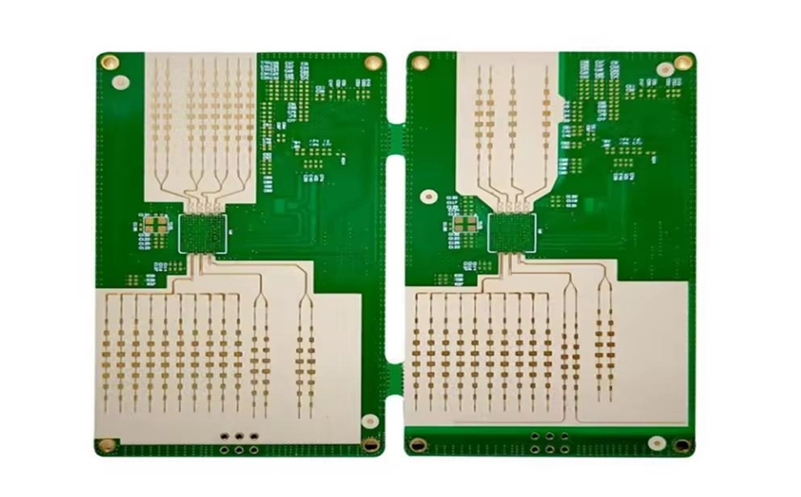
In today’s world, sustainability and energy efficiency are more important than ever. For engineers and designers working on printed circuit boards (PCBs), adopting low power PCB design strategies and using energy-efficient components can significantly reduce power consumption while contributing to eco-friendly practices. This blog dives deep into practical ways to achieve these goals, covering topics like reducing PCB power consumption, thermal management for green PCBs, and sustainable power distribution. Whether you’re designing for IoT devices or industrial systems, these tips will help you create efficient and environmentally conscious designs.
Why Energy Efficiency Matters in PCB Design
Energy-efficient PCB design isn’t just about saving power—it’s about meeting the growing demand for sustainable technology. With devices becoming smaller and more powerful, excessive power consumption leads to heat buildup, reduced lifespan, and higher environmental impact. By focusing on low power PCB design, you can minimize energy waste, lower operating costs, and contribute to a greener future. Let’s explore actionable strategies to make this happen.
Key Strategies for Low Power PCB Design
Designing a PCB with low power consumption requires careful planning and attention to detail. Below are some proven strategies to help you reduce energy usage without sacrificing performance.
1. Optimize Component Selection for Energy Efficiency
Choosing the right components is the foundation of energy-efficient PCB design. Opt for energy-efficient components like low-power microcontrollers (MCUs), voltage regulators, and sensors that operate at lower voltages, such as 1.8V or 3.3V instead of 5V. For example, modern MCUs often have sleep or idle modes that can cut power usage by up to 90% when the device isn’t active. Look for components with datasheets specifying low quiescent current (often in the microampere range, like 1-5 μA) to ensure minimal standby power draw.
Additionally, consider using power management integrated circuits (PMICs) to control and distribute power efficiently across the board. These chips can dynamically adjust voltage and current based on the load, reducing unnecessary energy waste.
2. Minimize Active Components and Simplify Circuits
The more active components on your PCB, the higher the power consumption. Simplifying your circuit by reducing the number of active elements, like transistors or amplifiers, can lower energy use. For instance, if a design can function with a single op-amp instead of two, you could cut power draw by nearly 50% in that section of the circuit. Use simulation tools to test and refine your design before manufacturing to ensure you’re not overcomplicating the layout.
3. Leverage Power-Saving Modes
Many modern components come with built-in power-saving modes, such as sleep, deep sleep, or standby. For example, a typical IoT device might consume 100 mW in active mode but only 10 μW in deep sleep. Designing your PCB to take advantage of these modes—by programming the firmware to switch to low-power states during idle periods—can drastically reduce overall power consumption. Ensure that your design includes proper wake-up mechanisms, like interrupts, to bring the system back to full operation when needed.
Reducing PCB Power Consumption Through Layout Techniques
Beyond component selection, the physical layout of your PCB plays a big role in energy efficiency. A well-thought-out layout can minimize power loss and improve performance. Here are some layout tips for reducing PCB power consumption.
1. Shorten Trace Lengths to Reduce Resistance
Long traces on a PCB create higher resistance, which leads to power loss as heat. By keeping traces as short as possible, especially for power lines, you can reduce voltage drops and energy waste. For instance, a trace with a resistance of 0.1 ohms carrying 1A of current will lose 0.1W of power as heat. Shortening that trace to lower the resistance to 0.05 ohms cuts the loss in half. Use wider traces for high-current paths to further minimize resistance.
2. Optimize Ground Planes for Efficient Current Return
A solid ground plane ensures a low-impedance path for return currents, reducing noise and power loss. Avoid splitting ground planes unnecessarily, as this can increase loop inductance and lead to inefficiencies. For high-frequency designs, a continuous ground plane can also help manage electromagnetic interference (EMI), which indirectly saves power by preventing signal degradation.
Thermal Management for Green PCBs
Heat is a byproduct of power consumption, and managing it effectively is crucial for both energy efficiency and sustainability. Poor thermal management can lead to higher power usage as components work harder under stress. Let’s look at some techniques for thermal management in green PCBs.
1. Use Heat Sinks and Thermal Vias
High-power components like voltage regulators or power transistors generate significant heat. Adding heat sinks to these components can dissipate heat more effectively, preventing thermal runaway where components consume more power due to rising temperatures. Thermal vias—small holes filled with conductive material—can also transfer heat from hot spots to other layers of the PCB or to an external heat sink. For example, placing 10-15 thermal vias under a power IC can reduce its operating temperature by 10-15°C, improving efficiency.
2. Choose Materials with Better Thermal Conductivity
The substrate material of your PCB affects how well it handles heat. Standard FR-4 material has a thermal conductivity of about 0.25 W/m·K, which isn’t ideal for high-power designs. Consider using materials like metal-core PCBs (MCPCBs) with thermal conductivity up to 1-4 W/m·K for better heat dissipation. While these materials may cost more, they can extend the lifespan of your PCB and reduce energy loss due to overheating.
Sustainable Power Distribution in PCB Design
Power distribution is another critical area for creating eco-friendly PCBs. Efficient power delivery reduces waste and ensures that every component gets the energy it needs without excess loss. Here are some tips for sustainable power distribution.
1. Implement Efficient Voltage Regulation
Using switch-mode power supplies (SMPS) instead of linear regulators can significantly boost efficiency. While linear regulators might have an efficiency of 30-50%, SMPS can achieve 85-95% efficiency by converting voltage with minimal heat loss. For a design requiring a step-down from 12V to 3.3V at 1A, an SMPS could save up to 6W of power compared to a linear regulator, directly reducing energy waste.
2. Distribute Power with Low-Loss Pathways
Design your power distribution network (PDN) to minimize voltage drops across the board. Place decoupling capacitors close to high-power components to stabilize voltage and reduce ripple, which can cause inefficiencies. For example, a 0.1 μF capacitor near an MCU can smooth out voltage spikes, ensuring the component operates at its optimal power level without drawing excess current.
Choosing Eco-Friendly Materials for Sustainable PCBs
Beyond power efficiency, the materials used in PCB manufacturing impact the environment. Traditional PCB production involves hazardous chemicals and non-recyclable materials, but newer options are making sustainable design more accessible.
1. Opt for Lead-Free and Halogen-Free Materials
Lead-free solder and halogen-free laminates reduce the environmental impact of PCBs. These materials comply with regulations like RoHS (Restriction of Hazardous Substances) and are less harmful during manufacturing and disposal. While lead-free solder may require slightly higher soldering temperatures (around 260°C versus 240°C for leaded solder), the trade-off is worth it for a greener design.
2. Explore Recyclable and Biodegradable Substrates
Some manufacturers are developing PCB substrates made from biodegradable or recycled materials, such as polylactic acid (PLA) composites. These alternatives may not yet match the performance of FR-4 in high-power applications, but they’re a promising option for low-power, eco-friendly designs. Using such materials can reduce landfill waste and lower the carbon footprint of your project.
Testing and Validation for Energy Efficiency
Once your PCB design is complete, testing is essential to ensure it meets energy efficiency goals. Use power analyzers to measure current draw across different operating modes. For example, if your design targets a standby current of 10 μA, verify this with precise measurements. Thermal imaging cameras can also help identify hot spots on the board, allowing you to adjust the layout or add cooling solutions before production.
Simulation software can predict power consumption and heat dissipation during the design phase. By running simulations with realistic load conditions, you can fine-tune your design to achieve optimal efficiency. For instance, simulating a circuit with a 500 mA load might reveal a voltage drop of 0.2V across a trace, prompting you to widen it for better performance.
Conclusion: Building a Greener Future with Energy-Efficient PCBs
Energy-efficient PCB design is a powerful way to reduce power consumption, manage heat, and contribute to sustainability. By focusing on low power PCB design, selecting energy-efficient components, optimizing layouts for reducing PCB power consumption, prioritizing thermal management for green PCBs, and ensuring sustainable power distribution, you can create designs that save energy and protect the environment. Start small by implementing one or two of these strategies in your next project, and gradually build toward fully eco-friendly designs. With these practices, you’re not just powering down your boards—you’re powering up a greener future.
 ALLPCB


