 ALLPCB


Aerospace electronics operate in environments that demand exceptional durability from every component, including printed circuit boards. Engineers must design these boards to handle rapid temperature swings, intense vibrations, radiation exposure, and pressure changes without compromising signal integrity or mechanical stability. The arrangement of conductive layers, dielectric materials, and vias plays a central role in achieving this performance. Proper stack-up configuration directly influences thermal management, electromagnetic compatibility, and long-term reliability in flight systems. Aerospace PCB designs therefore prioritize material compatibility and layer symmetry from the earliest stages of development.
Understanding PCB Stack-Up and Its Role in High-Reliability Applications
PCB stack-up refers to the precise layering of copper foils, prepregs, cores, and solder masks that form a multilayer board. In aerospace electronics this layering must accommodate differential coefficients of thermal expansion while maintaining consistent impedance across high-speed signals. The choice of dielectric constant, glass transition temperature, and copper weight affects how the board responds to extreme conditions. Engineers evaluate these parameters against operational requirements such as altitude-induced outgassing and mechanical shock. A well-planned stack-up reduces warpage and delamination risks that could otherwise lead to mission-critical failures.
Key Challenges Posed by Extreme Environmental Conditions
Aerospace platforms expose electronics to temperature cycles ranging from cryogenic levels at high altitude to elevated heat during re-entry or engine proximity. Vibration spectra from launch vehicles and rotorcraft can induce fatigue in copper traces and plated through-holes. Radiation effects further complicate material selection by potentially altering dielectric properties over time. Moisture absorption during ground storage followed by rapid depressurization creates additional stress on interfaces between layers. These combined factors require stack-up designs that balance electrical performance with mechanical robustness.
Related Reading: Aerospace PCB Conformal Coating: Meeting Stringent Requirements for Reliability
Technical Principles Governing Effective Stack-Up Design
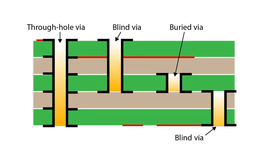
Symmetric layer arrangements help minimize residual stresses that develop during thermal cycling. Matching the coefficient of thermal expansion between copper and dielectric materials reduces the risk of cracking in vias and traces. Controlled impedance routing depends on precise dielectric thickness and copper etch tolerances that must remain stable across temperature extremes. Via structures such as blind, buried, or filled vias influence both signal integrity and thermal dissipation paths. Engineers apply finite-element analysis to predict how proposed stack-ups will behave under combined thermal and mechanical loads.
Related Reading: Aerospace PCB Design: Meeting AS9100 Standards for Reliability
Best Practices for Designing Aerospace PCB Stack-Up
Begin by selecting high-performance laminates with glass transition temperatures well above expected operating limits and low moisture absorption rates. Specify copper weights and foil types that support both current-carrying capacity and fine-line imaging requirements. Incorporate sufficient ground and power planes to provide shielding and heat spreading while preserving signal integrity. Use sequential lamination techniques when complex via configurations are necessary, ensuring each press cycle maintains registration accuracy. Validate the final stack-up through qualification testing aligned with established industry standards such as IPC-6012E.
Design reviews should include thorough review of drill-to-copper clearances and aspect ratios to prevent plating voids under thermal stress. Consider the placement of thermal vias and heat-spreading layers early in the layout process. Document all material specifications and process controls so that manufacturing remains consistent across production lots. These steps collectively support the creation of high-reliability PCB assemblies capable of surviving the full mission profile.
Conclusion
Effective PCB stack-up design forms the foundation for reliable aerospace electronics in extreme conditions. By addressing thermal, mechanical, and electrical requirements through symmetric construction, material compatibility, and rigorous validation, engineers can achieve the necessary performance margins. Continued attention to industry standards and qualification procedures ensures that designs translate successfully from prototype to flight hardware.
FAQs
Q1: What factors determine the optimal stack-up for aerospace PCB applications?
A1: Material selection, layer symmetry, and via configuration must align with temperature cycling, vibration, and radiation requirements typical of aerospace environments. Engineers evaluate dielectric properties and copper distribution to maintain signal integrity and mechanical stability throughout the mission profile.
Q2: How does PCB stack-up influence performance under extreme conditions?
A2: The arrangement of layers controls thermal expansion behavior, impedance consistency, and resistance to delamination when boards experience rapid temperature changes and mechanical shock. Proper stack-up reduces stress concentrations that could otherwise compromise high-reliability PCB assemblies.
Q3: Why is layer symmetry important in aerospace electronics stack-up?
A3: Symmetric construction minimizes warpage and residual stresses during thermal cycling, helping plated through-holes and traces remain intact under repeated expansion and contraction. This approach supports long-term reliability in aerospace PCB designs subjected to altitude and temperature extremes.
Q4: What role do industry standards play in aerospace PCB stack-up qualification?
A4: Standards such as JEDEC J-STD-020E guide moisture sensitivity and reflow testing that verify stack-up robustness before deployment. Compliance ensures consistent manufacturing processes and predictable behavior in extreme operating environments.


