If you're looking to understand the PCB inner layer etching process, the role of etching chemicals, and the importance of photoresist stripping, you've come to the right place. At ALLPCB, we know that precision in etching is critical for creating high-quality multilayer printed circuit boards (PCBs). In this blog, we’ll dive deep into the techniques, chemicals, and control methods that ensure accurate inner layer etching, helping engineers and manufacturers achieve reliable results every time.
Inner layer etching is a foundational step in PCB manufacturing, especially for multilayer boards where internal conductive layers form complex circuits. This process requires meticulous control to avoid defects like over-etching or under-etching, which can compromise signal integrity or board functionality. Below, we’ll explore every aspect of this process, from the basics to advanced precision techniques, to give you a complete guide for optimizing your PCB production.
What Is PCB Inner Layer Etching?
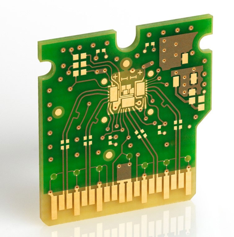
PCB inner layer etching is the process of removing unwanted copper from the internal layers of a multilayer PCB to create the desired circuit patterns. Unlike outer layers, inner layers are embedded within the board, making precision even more critical since errors cannot be easily corrected once the layers are laminated together. This process relies on chemical reactions to dissolve copper, guided by a protective mask called photoresist, which defines the circuit design.
The goal of inner layer etching is to achieve clean, accurate traces with minimal deviation from the design specifications. For example, a typical inner layer trace width might be as narrow as 4 mils (0.004 inches), requiring etching precision within ±0.5 mils to maintain signal integrity at high frequencies, such as 5 GHz for RF applications. Any deviation could lead to impedance mismatches or signal loss, affecting the board's performance.
Why Precision Matters in Inner Layer Etching
Precision in inner layer etching directly impacts the reliability and functionality of a PCB. Multilayer boards often have 4 to 16 layers (or more in advanced designs), and each layer must align perfectly during lamination. If etching is uneven or inaccurate, it can cause issues like:
- Short Circuits: Over-etching can remove too much copper, narrowing traces and risking breaks or shorts.
- Signal Integrity Issues: Inconsistent trace widths can alter impedance, critical for high-speed signals (e.g., 50 ohms for many digital applications).
- Manufacturing Delays: Defects in inner layers often mean scrapping the entire board, as rework is nearly impossible post-lamination.
The PCB Inner Layer Etching Process: Step by Step
The PCB inner layer etching process involves several carefully controlled steps to ensure the copper is removed only from unwanted areas. Let’s break down the process to understand how precision is achieved at each stage.
1. Inner Layer Material Preparation
The process starts with a copper-clad laminate, typically a thin layer of copper (e.g., 1 oz or 0.0014 inches thick) bonded to a dielectric substrate like FR-4. For multilayer boards, these laminates will form the internal layers. The surface is cleaned to remove contaminants like oils or oxides, ensuring proper adhesion of the photoresist in the next step.
2. Photoresist Application
A light-sensitive material called photoresist is applied to the copper surface. This can be done using a liquid coating or a dry film, with dry film being more common for inner layers due to its uniform thickness (typically 1.5 mils). The photoresist acts as a protective mask during etching, shielding the copper that will form the circuit traces.
3. Imaging and Exposure
The circuit design is transferred to the photoresist using a photolithographic process. A film or digital mask with the circuit pattern is aligned over the photoresist, and UV light is used to expose it. Areas exposed to light harden (in negative photoresist), while unexposed areas remain soluble and are later removed during development.
4. Development
After exposure, the board is immersed in a developer solution, usually a mild alkaline chemical like sodium carbonate. This removes the unexposed photoresist, leaving behind a pattern that exposes the copper to be etched away while protecting the areas that will become traces.
5. Etching with Chemicals
Here’s where the etching chemicals come into play. The board is submerged in or sprayed with an etchant solution that dissolves the exposed copper. Common etchants include:
- Cupric Chloride (CuCl2): Widely used for its fast etching rate and ability to be regenerated, reducing waste. It operates at temperatures around 50°C and can etch copper at a rate of 1 mil per minute.
- Ammoniacal Etchant: An alkaline solution often used for finer lines due to its controllable etch rate, though it requires careful handling due to ammonia fumes.
- Ferric Chloride (FeCl3): A traditional etchant, less common today due to disposal challenges, but still used in smaller-scale operations.
The etching process must be tightly controlled for time, temperature, and chemical concentration to avoid over-etching (removing too much copper) or under-etching (leaving residual copper). For instance, a deviation of just 2°C in temperature can alter the etch rate by 10%, affecting trace uniformity.
6. Photoresist Stripping
Once etching is complete, the remaining photoresist is removed in a process called photoresist stripping. This typically involves a strong alkaline solution, such as sodium hydroxide, which dissolves the hardened photoresist without damaging the copper traces. Proper stripping is crucial; any leftover resist can interfere with subsequent processes like lamination or plating, leading to defects.
Key Factors for Precision in Inner Layer Etching
Achieving precision in the PCB inner layer etching process requires careful control of multiple variables. Below are the critical factors that manufacturers must monitor to ensure high-quality results.
Chemical Concentration and Temperature
The concentration of etching chemicals directly affects the speed and uniformity of copper removal. For example, a cupric chloride solution with a specific gravity of 1.2 to 1.3 is often ideal for consistent etching. Temperature also plays a role; most etchants work best between 45°C and 55°C. Automated systems with real-time monitoring can adjust these parameters to maintain a stable etch rate, ensuring trace widths remain within tolerances like ±0.2 mils for fine-pitch designs.
Etching Time
Overexposure to etchant can lead to undercutting, where the chemical eats away at the sides of traces, narrowing them beyond the intended design. For a 1 oz copper layer, etching might take 2-3 minutes with cupric chloride under optimal conditions. Advanced manufacturing setups use conveyorized etching machines with precise timers to stop the process at the exact moment.
Photoresist Quality and Alignment
The photoresist must be applied evenly and aligned perfectly with the design mask. Misalignment as small as 1 mil can result in shifted traces, causing issues in multilayer stack-ups where vias must connect across layers. High-resolution imaging systems and automated optical inspection (AOI) help detect and correct alignment errors before etching begins.
Uniformity of Etchant Application
Uneven application of etchant, whether through immersion or spray, can lead to inconsistent etching across the board. Spray etching systems are often preferred for inner layers because they provide uniform chemical distribution and allow better control over etch rates. Regular maintenance of nozzles and pumps ensures consistent performance.
Common Challenges in Inner Layer Etching and Solutions
Even with advanced equipment, challenges in inner layer etching can arise. Here are some common issues and how to address them for optimal results.
Over-Etching and Undercutting
Over-etching occurs when the copper is exposed to etchant for too long, resulting in narrower traces or even breaks. Undercutting worsens this by eroding the sides of traces. To prevent this, manufacturers use etch factor calculations—a ratio of vertical to lateral etching, ideally kept above 2:1 for fine lines. Automated etching systems with endpoint detection can stop the process precisely when the exposed copper is removed.
Under-Etching and Residual Copper
Under-etching leaves unwanted copper on the board, risking short circuits. This often happens due to insufficient etchant strength or uneven application. Regular testing of chemical solutions and the use of agitation during etching can ensure complete copper removal. AOI systems can also detect residual copper post-etching for immediate correction.
Photoresist Stripping Issues
Incomplete photoresist stripping can leave residue that interferes with later processes. Using the correct stripping solution concentration (e.g., 2-5% sodium hydroxide) and ensuring adequate rinse cycles can prevent this. Ultrasonic cleaning may also be employed for stubborn residues, though it must be carefully controlled to avoid damaging delicate traces.
Advanced Techniques for Precision Control
As PCB designs become more complex, with finer traces (down to 2 mils) and higher layer counts (up to 24 or more), advanced techniques are essential for maintaining precision in inner layer etching.
Real-Time Monitoring and Automation
Modern etching lines integrate sensors to monitor temperature, chemical concentration, and etch rate in real time. Machine learning algorithms can predict and adjust parameters to maintain consistency, reducing defect rates to below 1% in high-volume production. This is especially critical for applications like aerospace or medical devices, where reliability is non-negotiable.
Dry Etching for Ultra-Fine Features
While wet etching with chemicals is standard, dry etching using plasma is gaining traction for ultra-fine features below 1 mil. Plasma etching offers superior control and minimal undercutting, though it’s more expensive and typically reserved for high-end applications like advanced IC substrates.
Environmentally Friendly Etchants
Sustainability is a growing concern in PCB manufacturing. Regenerable etchants like cupric chloride reduce waste by allowing the chemical to be reused after copper recovery. Additionally, alternatives to ferric chloride, such as sodium persulfate, are being explored for their lower environmental impact, though they require careful handling for consistent results.
Conclusion: Mastering PCB Inner Layer Etching for Quality Results
The PCB inner layer etching process is a cornerstone of multilayer PCB manufacturing, demanding precision at every step—from photoresist application to etching with the right etching chemicals and thorough photoresist stripping. By understanding the process and implementing strict control over variables like chemical concentration, temperature, and timing, manufacturers can achieve the tight tolerances needed for modern electronics, whether it’s a 4-layer board for consumer devices or a 16-layer design for high-speed computing.
At ALLPCB, we’re committed to delivering top-tier PCB solutions by leveraging advanced etching techniques and rigorous quality control. Whether you’re designing for standard applications or pushing the boundaries with fine-pitch traces, mastering inner layer etching ensures your boards perform reliably under any conditions. With the insights shared in this guide, you’re equipped to optimize your PCB production process for precision and efficiency.
 ALLPCB


