ALLPCB


Size and efficiency challenges for wearables
For wearable devices, small size is a primary factor when selecting components, including those used for power supplies. DC/DC converters offer high conversion efficiency and, by integrating the controller and key passive components into system-in-package (SiP) modules, they minimize printed circuit board area, help reduce device size, and simplify layout. This article examines how packaging integration reduces the size of switching converters for wearable devices and the design considerations involved.
Wearable design presents many challenges, and one key requirement is power efficiency in the context of form factor. Devices worn for extended periods need good battery autonomy. Because these devices are close to the skin, efficient converters are preferred, which switching power supplies can provide instead of traditional low-dropout linear regulators. However, switching-mode designs are more complex. While CMOS integration lets active elements such as on-chip power transistors shrink, traditional DC/DC converter designs assume external passive components. Those discrete parts may be compact individually, but when combined to support converter operation they can occupy substantial PCB area compared with the main SoC.
Larger portable designs have historically tolerated the PCB area required for power circuits. Wearable form factors demand the largest possible battery capacity between charges, which increases pressure on space allocated to other system components.
Minimizing PCB area and managing noise
In addition to high conversion efficiency, DC/DC converters for wearables must minimize PCB area by using fewer devices or packing more devices into smaller spaces. Reduced size imposes constraints on PCB layout: it becomes harder to move components to minimize noise and parasitics or to isolate other sensitive parts of the system. Low-noise components and topologies are therefore needed to ensure that efficient switching techniques do not disturb other design elements.
Advances in materials and manufacturing for passives such as capacitors and inductors have enabled reductions in overall size. To conserve PCB area, manufacturers such as Murata, Texas Instruments and Torex have adopted system-in-package technology to further shrink the required area. In some cases these solutions integrate the controller IC, the inductor, and capacitors within the same package.
SiP benefits and layout options
SiP technology allows components to be integrated into IC-compatible packages. Shorter interconnects and fine-pitch redistribution layers used inside the package reduce inductance and capacitance, and the solder pads used on the SiP are much smaller than the pads needed on the PCB for discrete components.
Although SiP reduces the space required for a power converter, designers must still choose among package topologies because a single SiP layout cannot satisfy all system requirements. A key issue is the placement of the inductor inside the package, which is why some vendors offer multiple SiP configurations. Typical choices include covering the controller IC with the inductor, stacking the controller IC on top of the inductor, or placing the IC and inductor side by side. The package structure is determined by product specifications, IC and inductor characteristics, thermal performance, and other factors.
Covering the controller IC with the inductor generally offers the best performance for radiated noise and magnetic emissions, and the stack reduces PCB area. Stacking the controller IC on top of the inductor can lower cost because wire bonding to the raised IC pads is a cost-effective technique for stacked topologies. When the controller IC is covered by the inductor, the same bonding techniques may not be available. That covered configuration increases magnetic field strength near the PCB, so it is unsuitable for designs that are sensitive to nearby magnetic fields. Radiated noise is also slightly higher compared with the inverted configuration. Thermal performance can worsen because a thermal pad cannot be connected to the bottom of the controller IC to remove heat via the PCB, and heat tends to flow between stacked elements.
Placing the IC and the inductor side by side increases PCB area, although the more efficient SiP pad layout still reduces the overall footprint compared with placing passive components discretely on the PCB. This arrangement offers the best heat dissipation, relatively low cost, and improved compatibility with magnetic-field-sensitive designs. However, noise performance can be better in certain stacked configurations.
Compared with discrete implementations, micro converters in SiP form often show improved noise performance because of shorter interconnects. Off-the-shelf SiP designs also reduce the number of layout decisions required from PCB designers, helping accelerate development. The main layout considerations are the arrangement and routing of ground and power connections to minimize parasitics.
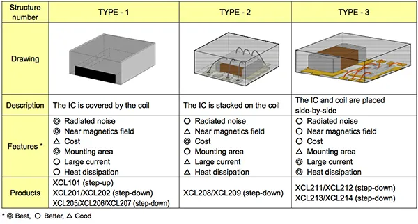
Figure 1: SiP configuration options for micro converters. (Provided by Torex)
Vendor examples and package details
Torex's XCL201, XCL202, XCL205 and XCL206 are synchronous step-down DC/DC converters that integrate the inductor in a top-inductor format. The entire SiP, including the inductor, occupies 2.5 mm × 2.0 mm of PCB area. To limit the combined coil and DC/DC height to 1.0 mm, the DC/DC IC uses a new 0.4 mm high ultra-flat package. Similar devices XCL208 and XCL209 use a simpler package that places the inductor beneath the DC/DC device to reduce production cost. XCL208 and XCL209 also provide adjustable output voltage options, while XCL201 and XCL202 show roughly 3% improved power efficiency across most load conditions. To reduce the core converter package size, two external capacitors are required.
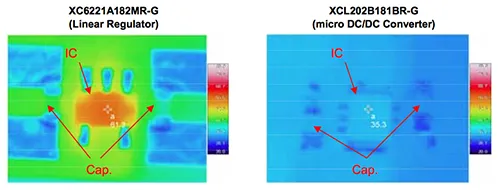
Figure 2: Thermal comparison between traditional linear converters and SiP micro converters. (Provided by Torex)
Murata's LXDC series includes DC/DC micro converters that offer internal or external capacitors. To minimize the core SiP size, the LXDC2HL requires two external capacitors, but the package measures 2.5 mm × 2.0 mm and uses an embedded ferrite substrate to form the inductor element. The connection length between the controller IC and the inductor is effectively zero, which helps reduce noise emissions. Ferrite multilayer substrate technology stacks up to 50 layers of different ferrite materials to create three-dimensional circuitry within the device substrate.
Buck converter devices are typically designed for 2.3 V to 5.5 V supplies such as lithium-ion batteries. Murata's 2UR and 3EP series integrate input and output capacitors on the ferrite substrate: this increases package size slightly but saves more PCB area when integrated. The 3EP overall package is larger at 3.5 mm × 3.2 mm but offers improved efficiency—about 2% higher—and a 1 A maximum load compared with 600 mA for the 2UR. Although the 2UR package includes capacitors, its PCB footprint is only slightly larger than the 2HL version at 2.5 mm × 2.3 mm. Murata's micro converters use an open-frame structure to enhance thermal performance.
Texas Instruments' TPS82740 packages a buck converter into a 2.9 mm × 2.3 mm SiP that includes the necessary passive components arranged on the top surface in an open-frame, surface-mount configuration. The micro regulator can switch from pulse-width modulation (PWM) to pulse-frequency modulation (PFM) for light-load efficiency. TPS82740 uses a control scheme that reduces quiescent current to 360 nA. In PWM mode it supports up to 200 mA output current, and it switches to a low-power pulse mode when the load falls below 10 μA.
The TPS82740's DCS control mechanism combines hysteresis and voltage-mode control. The controller builds around an AC loop that senses output voltage. Comparators use that voltage to set the switching frequency, which remains constant under steady-state conditions while providing immediate response to dynamic load changes. A voltage feedback loop is used for accurate DC load regulation. When load current decreases, the converter enters a power-save mode to improve efficiency, and switching frequency varies nearly linearly with load current. In pulse mode, the device issues a switching pulse to boost inductor current and recharge output capacitors, followed by a sleep period during which most internal circuits are shut down to reduce current consumption. During this interval, the output capacitors supply the load current.
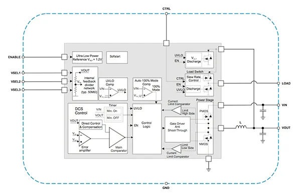
Figure 3: Block diagram of TI TPS82740.
Summary
Advances in SiP packaging and control algorithms enable compact, low-noise DC/DC converter solutions that free PCB space for larger batteries and improve overall energy efficiency. These developments support longer run times and smaller form factors for the next generation of wearable devices.