 ALLPCB


Introduction
In the competitive landscape of electronics manufacturing, optimizing PCB layout and design is crucial for achieving streamlined mass production. Design for manufacturing principles ensure that boards transition smoothly from prototyping to high-volume runs, minimizing defects and production costs. Electric engineers must prioritize component placement guidelines, signal integrity considerations, thermal management solutions, and rigorous design rule checks to meet these goals. Poor layout choices can lead to assembly challenges, yield losses, and reliability issues in mass production environments. By integrating these elements early in the design phase, teams can enhance manufacturability while maintaining performance standards. This article explores structured approaches to create PCBs ready for efficient scaling.
Understanding Design for Manufacturing Principles in PCBs
Design for manufacturing principles, often abbreviated as DFM, encompass guidelines that align PCB design with fabrication and assembly capabilities. These principles focus on simplifying processes to boost yield rates and reduce cycle times in mass production. For instance, standardizing features like hole sizes and trace spacings prevents custom tooling needs that inflate costs. Engineers apply DFM by considering the entire supply chain, from material selection to final testing. Adhering to IPC-2221 Generic Standard on Printed Board Design helps establish baseline requirements for conductor sizing, spacing, and overall board geometry. Ultimately, DFM transforms complex designs into producible realities, supporting consistent quality across thousands of units.
Mass production amplifies the impact of DFM decisions, as even minor flaws multiply expenses exponentially. Boards designed without these principles often face issues like warpage, solder joint failures, or impedance mismatches during scaling. Proactive DFM integration allows for panelization, where multiple boards share a single panel for parallel processing. This approach optimizes material usage and throughput in automated lines. Engineers benefit from logical structuring that anticipates reflow soldering, inspection, and test fixture compatibility. The result is higher first-pass yields and faster time-to-market for volume orders.
Component Placement Guidelines for Optimal Assembly Flow
Component placement guidelines form the foundation of efficient PCB layouts, directly influencing assembly speed and defect rates. Engineers should group components by function, such as placing all power regulators together to shorten traces and ease thermal clustering. Prioritize edge placement for connectors and heavy parts to facilitate handling and prevent board stress during handling. In surface-mount technology dominant mass production, orient parts consistently for pick-and-place machines, aligning polarities and minimizing rotations. Maintain adequate spacing around tall components to avoid shadowing during reflow soldering. These guidelines reduce programming time for automated equipment and improve inspection visibility.
Logical placement also supports signal flow, positioning high-speed signals centrally while isolating analog sections from digital noise sources. For mass runs, avoid placing fine-pitch devices near board edges where handling risks damage. Balance the board to prevent warpage from uneven component density, distributing mass symmetrically across layers. Component placement guidelines extend to fiducial marks, which must be clear and symmetrically placed for precise alignment in vision systems. By following these practices, designs achieve higher assembly yields and lower rework needs. Electric engineers can simulate placement impacts using basic flow analysis to validate choices pre-layout.
Related Reading: Panelization Strategies for High Density PCB Assembly: Overcoming Component Placement Challenges
Signal Integrity Considerations for High-Volume Reliability
Signal integrity considerations are paramount in modern PCBs, especially as operating frequencies rise in mass-produced devices. Engineers must route critical signals with controlled impedance, using consistent widths and avoiding sharp bends that cause reflections. Matched-length routing for differential pairs prevents skew, ensuring data integrity across high-speed buses. Layer stacking plays a key role, with signal layers adjacent to ground planes to minimize crosstalk and EMI. In mass production, these considerations prevent field failures by standardizing routing patterns that scale reliably. Design rule checks verify minimum clearances and via usage to maintain performance uniformity.
Crosstalk mitigation involves shielding sensitive traces and staggering parallel runs to reduce coupling. Engineers address via stubs by back-drilling where necessary, though this adds cost, so plan strategically for volume. Signal integrity simulations complement layout efforts, but physical DRC enforces baseline compliance. For multilayer boards, assign inner layers thoughtfully to separate power and signals. These practices ensure boards meet performance specs lot-to-lot. Integrating signal integrity early avoids costly respins in production ramps.
Thermal Management Solutions in Dense PCB Designs
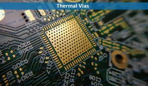
Thermal management solutions address heat dissipation challenges inherent in densely packed mass-produced PCBs. Engineers distribute heat-generating components evenly, avoiding hotspots that warp boards or degrade solder joints. Copper pours and planes act as heat spreaders, connected via thermal vias arrays under ICs. Via tents and plugs prevent solder wicking while enabling efficient heat transfer to inner layers. Placement guidelines position sensitive parts away from primary heat sources, with airflow paths in mind for enclosed systems. These solutions maintain junction temperatures within operational limits across production variations.
Advanced thermal management incorporates embedded vias in pads and staggered via fields for better airflow. Engineers use thicker copper in power sections for inherent spreading, balanced against etching yields. Design rule checks enforce via annular rings and spacing to prevent shorts during reflow. For high-power applications, outline cutouts or slots enhance convection without compromising strength. Consistent application ensures reliability in volume manufacturing. Thermal profiling during design validates solutions before commitment.
Related Reading: The Ultimate Guide to PCB Thermal Management: Techniques, Materials, and Design
Design Rule Checks for Manufacturing Compliance
Design rule checks serve as the gatekeeper for manufacturable layouts, automating verification of spacing, widths, and overlaps. Engineers configure DRC to enforce minimum trace-to-trace distances, pad-to-pad clearances, and annular ring sizes per fabricator capabilities. These checks catch violations early, preventing etch failures or shorts in mass production. Layer-specific rules address via breakout, drill sizes, and solder mask expansion. Running DRC iteratively refines the layout, integrating feedback from DFM reviews. Comprehensive checks include panelization rules for v-scoring and tab routing.
Beyond electrical rules, DRC validates mechanical aspects like keep-out zones around fiducials and tooling holes. Engineers prioritize rules aligned with IPC-A-600 Acceptability of Printed Boards for visual and dimensional criteria. Netlist comparisons ensure schematic-to-layout fidelity. For signal integrity, DRC flags impedance deviations and length mismatches. These systematic checks streamline reviews and boost confidence in production readiness. Regular DRC discipline minimizes engineering change orders downstream.
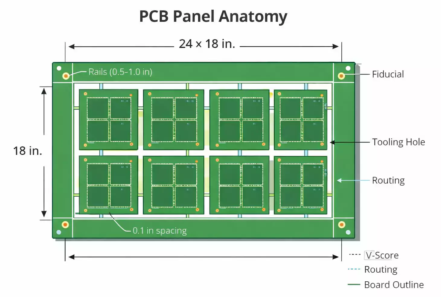
Best Practices for Panelization and Mass Production Scaling
Panelization best practices enable efficient material use and parallel processing in mass production. Engineers array identical boards with 5-10mm spacing, incorporating fiducials at corners and centers for alignment. Tooling holes, sized to standard drills, support fixturing without custom punches. V-grooves or mouse bites define break lines, balancing strength and ease of depaneling. Component placement guidelines extend to panels by avoiding edges near rails. These practices cut per-board costs significantly at volume.
Symmetrical panel design prevents warpage from thermal mismatch during lamination and reflow. Engineers verify rail widths accommodate handling equipment. For mixed assemblies, standardize stencil apertures across the array. Post-DRC, perform DFM analysis for drill hit counts and aspect ratios. Implementing these ensures smooth ramp-up to thousands of units daily. Collaboration with production teams refines panel configs iteratively.
Conclusion
Optimizing PCB layout and design through design for manufacturing principles unlocks streamlined mass production potential. Component placement guidelines, signal integrity considerations, thermal management solutions, and design rule checks form an interconnected framework for success. Electric engineers who structure layouts logically achieve higher yields, lower costs, and reliable performance. Standards like IPC-2221 and IPC-A-600 provide essential guardrails without overcomplicating designs. Prioritizing these elements early pays dividends in scalable manufacturing. Ultimately, thoughtful design bridges innovation and production efficiency seamlessly.
FAQs
Q1: What are the core design for manufacturing principles for PCBs?
A1: Design for manufacturing principles emphasize standardized features like trace spacings, hole sizes, and fiducials to align with fabrication limits. They prioritize symmetry to avoid warpage and logical component grouping for assembly flow. Engineers apply these to boost yields in mass production, reducing custom processes. Following IPC-2221 ensures conductor and spacing compliance. These principles cut costs and cycle times effectively.
Q2: How do component placement guidelines impact mass PCB production?
A2: Component placement guidelines optimize for pick-and-place efficiency by grouping functions and balancing mass distribution. They minimize trace lengths for signal integrity and isolate heat sources. In mass runs, consistent orientation speeds programming and inspection. Avoiding edge placement for fine-pitch parts prevents damage. These guidelines directly enhance throughput and yield rates.
Q3: Why are signal integrity considerations critical in high-volume layouts?
A3: Signal integrity considerations prevent reflections, crosstalk, and EMI through controlled routing and layer planning. Matched lengths and impedance control ensure performance consistency across lots. DRC enforces these to avoid field failures. In volume production, they standardize designs for reliable scaling. Engineers integrate them to maintain data speeds without respins.
Q4: What role do design rule checks play in thermal management solutions?
A4: Design rule checks verify via spacing, copper thicknesses, and clearances for effective heat spreading. They flag overlaps that could cause shorts in thermal vias. Checks align with standards for pad reliefs and pours. This ensures thermal solutions perform reliably in mass production. Comprehensive DRC upholds solution integrity throughout layout.


