 ALLPCB


If you're looking to optimize your PCB design for efficient assembly and reduced production costs, understanding DFA (Design for Assembly) guidelines for component spacing is essential. Proper spacing ensures smooth automatic assembly, minimizes rework, and enhances overall board reliability. In this guide, we'll dive into the specifics of DFA guidelines for component spacing, including minimum component distance on PCBs, component-to-edge spacing, and spacing considerations for rework and automatic assembly. Let's explore how to master these principles for better designs and seamless manufacturing.
Why Component Spacing Matters in PCB Design
Component spacing is a critical aspect of PCB design that directly impacts the ease of assembly, the risk of manufacturing defects, and the long-term reliability of the board. When components are placed too close together, issues like solder bridging, interference during automated assembly, and difficulty in rework can arise. On the other hand, overly generous spacing can waste valuable board real estate, increasing costs and limiting design efficiency.
By following DFA guidelines for component spacing, designers can strike the right balance. These guidelines are tailored to streamline the assembly process, whether done manually or through automated pick-and-place machines, while ensuring the board remains functional and durable. For engineers and designers, adhering to these rules means fewer production delays, lower costs, and higher-quality outcomes.
What Are DFA Guidelines and Why Are They Important?
DFA, or Design for Assembly, refers to a set of design practices aimed at making a product easier and more cost-effective to assemble. In the context of PCB design, DFA guidelines focus on optimizing component placement, orientation, and spacing to minimize assembly errors and reduce manufacturing time. These principles are especially crucial in high-volume production, where small inefficiencies can lead to significant costs.
The importance of DFA lies in its ability to prevent common assembly issues. For instance, improper spacing can cause components to interfere with each other during placement or soldering, leading to defects. DFA guidelines help designers avoid such problems by providing clear rules for minimum distances, orientations, and edge clearances. By integrating these practices into your workflow, you can achieve a smoother assembly process and a more reliable final product.
Key DFA Guidelines for Component Spacing on PCBs
Let’s break down the core DFA guidelines related to component spacing. These rules are designed to address various aspects of PCB assembly, from automated processes to manual rework. We'll cover minimum component distances, component-to-edge spacing, and specific considerations for automatic assembly and rework.
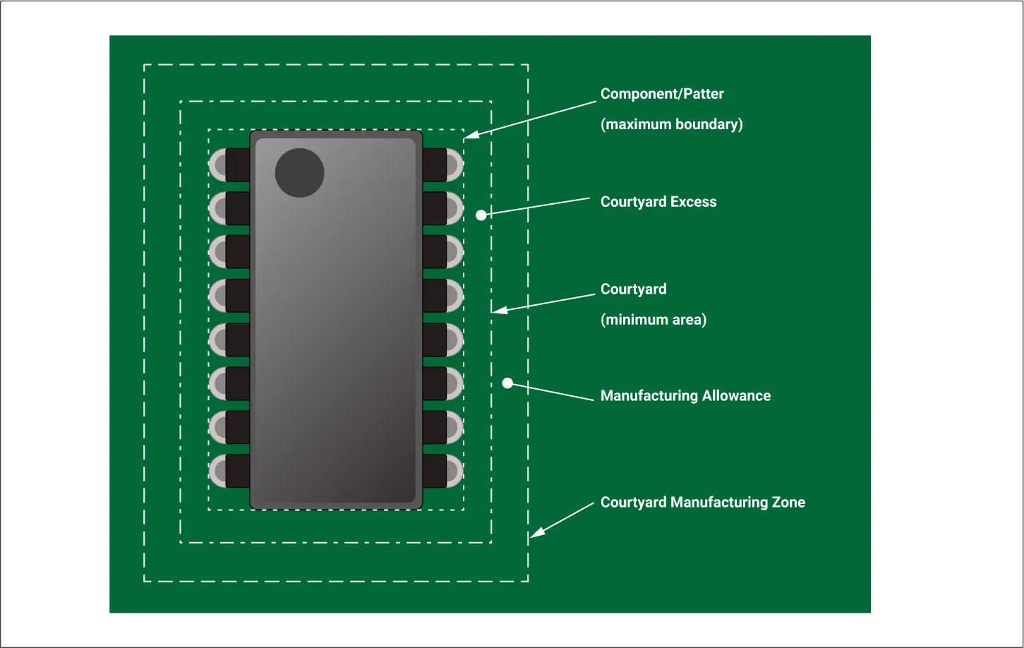
1. Minimum Component Distance on PCBs
The minimum distance between components on a PCB is a fundamental DFA guideline. This spacing ensures that components do not interfere with each other during assembly or soldering. While the exact distance can vary based on the type of components and assembly method, a general rule of thumb is to maintain at least 0.5 mm of clearance between components. For high-density designs, a slightly larger clearance of 0.8 mm is often recommended to provide extra safety.
This spacing prevents issues like solder bridging, where excess solder connects adjacent pads, causing short circuits. It also allows enough room for automated pick-and-place machines to position components accurately without collision. For larger components or those with heat dissipation requirements, such as power transistors, a greater distance—often 1.5 mm or more—may be necessary to manage thermal stress and ensure proper airflow.
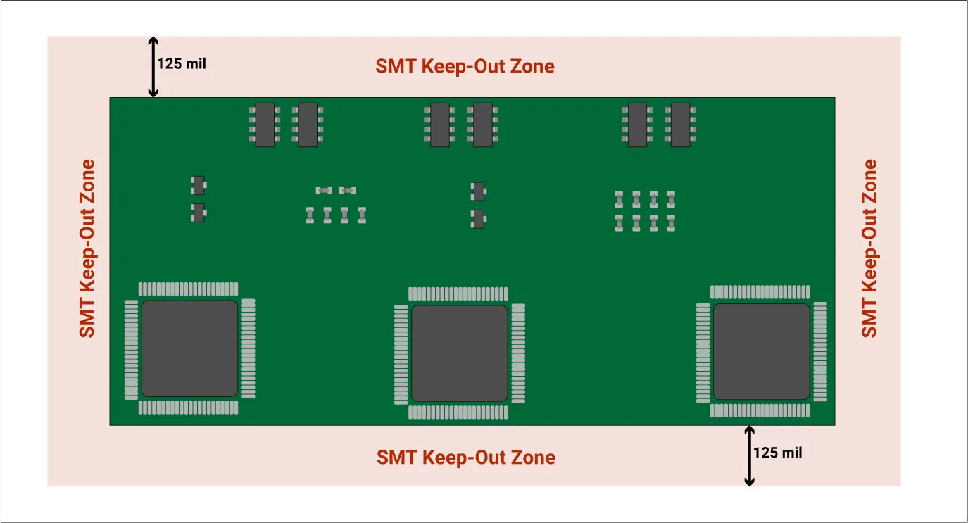
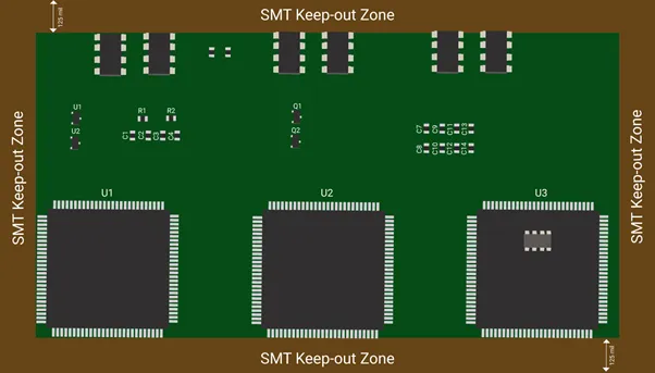
2. Component-to-Edge Spacing in DFA
Component-to-edge spacing is another critical factor in DFA guidelines. Keeping components away from the edges of the PCB protects them during handling, assembly, and testing processes. A common recommendation is to maintain at least 3 mm of clearance between components and the board's edge. This distance helps prevent damage to components during depanelization (the process of separating individual boards from a larger panel) and reduces the risk of mechanical stress.
For automated assembly, edge clearance is particularly important as it ensures that robotic arms and other machinery can operate without accidentally damaging components near the perimeter. Additionally, this spacing provides room for test fixtures and connectors that may need to interface with the board during manufacturing or quality control.
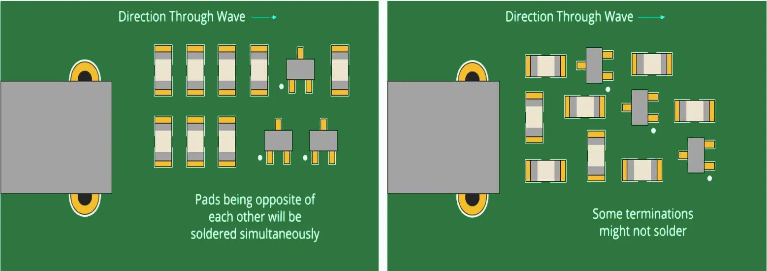
3. Spacing for Automatic Assembly
Automatic assembly, typically performed using pick-and-place machines, requires precise component spacing to ensure accuracy and efficiency. DFA guidelines for automatic assembly emphasize uniform orientation and adequate clearance to simplify machine programming and operation. For instance, resistors, capacitors, and ICs should be placed in the same orientation whenever possible to reduce the need for machine recalibration.
In terms of spacing, a minimum clearance of 0.5 mm between components is often sufficient for most automated systems. However, for high-speed assembly lines or designs with very small components, increasing this to 0.8 mm can help avoid placement errors. Additionally, designers should avoid placing components in areas where machine vision systems or robotic arms might struggle to access them, such as near tall components that could cast shadows or obstruct movement.
4. Spacing for Rework Considerations
Rework refers to the process of repairing or replacing components on a PCB after initial assembly, often due to defects or design changes. DFA guidelines for spacing in rework scenarios focus on providing enough room for technicians to access components without damaging nearby parts. A minimum spacing of 1.0 mm to 1.5 mm between components is typically recommended for rework, as it allows space for soldering irons, desoldering tools, and other equipment.
For surface-mount components, which are common in modern designs, rework spacing is especially important. These components are small and delicate, and insufficient clearance can lead to accidental damage during repair. Designers should also consider placing test points or access areas near critical components to facilitate troubleshooting and rework without compromising the board’s layout.
Practical Tips for Implementing DFA Component Spacing Guidelines
Now that we’ve covered the core DFA guidelines for component spacing, let’s look at some practical tips to help you apply these principles effectively in your PCB designs. These tips are geared toward engineers and designers who want to optimize their layouts for manufacturability and reliability.
Tip 1: Use Design Software with DFA Checks
Many modern PCB design tools come with built-in DFA checks that can automatically flag spacing violations. These features analyze your layout against standard guidelines, such as minimum component distance and edge clearance, and alert you to potential issues before you send the design for manufacturing. Leveraging these tools can save time and reduce the risk of costly errors during assembly.
Tip 2: Prioritize Component Grouping
Group similar components together in your layout to simplify assembly and reduce spacing issues. For example, place all capacitors in one area and resistors in another, maintaining consistent spacing within each group. This approach not only improves the efficiency of automated assembly but also makes the board easier to inspect and rework if needed.
Tip 3: Account for Manufacturing Tolerances
Manufacturing tolerances can affect how components are placed and soldered on a PCB. When determining spacing, consider the tolerances of your assembly process, such as the accuracy of pick-and-place machines (typically ±0.1 mm for high-end systems). Adding a small buffer to the minimum spacing requirements can help accommodate these variations and prevent assembly defects.
Tip 4: Test Your Design with Prototypes
Before moving to full-scale production, create prototypes of your PCB design to test component spacing under real-world assembly conditions. Prototyping allows you to identify potential issues, such as insufficient clearance for rework or automated placement errors, and make adjustments before committing to a large manufacturing run.
Common Mistakes to Avoid in Component Spacing
Even with the best intentions, designers can make mistakes when applying DFA guidelines for component spacing. Here are some common pitfalls to watch out for and how to avoid them.
Mistake 1: Ignoring Edge Clearance
Placing components too close to the edge of the PCB can lead to damage during handling or depanelization. Always adhere to the recommended 3 mm clearance to protect components and ensure smooth manufacturing.
Mistake 2: Overcrowding Components
In an effort to save space, designers sometimes place components too close together, violating minimum spacing rules. This can cause solder bridging and assembly errors. Stick to the 0.5 mm to 0.8 mm clearance guidelines to maintain reliability.
Mistake 3: Neglecting Rework Needs
Failing to account for rework spacing can make repairs difficult or impossible without damaging nearby components. Plan for at least 1.0 mm of clearance around components that are likely to require rework, such as high-failure-rate parts.
The Benefits of Mastering DFA Component Spacing
By mastering DFA guidelines for component spacing, you can unlock several benefits for your PCB designs. First, proper spacing reduces the likelihood of assembly errors, leading to fewer defects and lower production costs. Second, it enhances the reliability of the final product by minimizing issues like solder bridging and mechanical stress. Finally, adhering to these guidelines streamlines the manufacturing process, whether you're using automated assembly or manual rework, resulting in faster turnaround times and happier clients.
For engineers and designers, investing time in understanding and applying DFA principles is a smart move. It not only improves the quality of your designs but also positions you as a professional who prioritizes manufacturability and efficiency.
Conclusion: Elevate Your PCB Designs with DFA Guidelines
Component spacing is a cornerstone of effective PCB design, and following DFA guidelines ensures that your boards are optimized for assembly, rework, and long-term reliability. By maintaining minimum component distances, respecting edge clearances, and planning for automatic assembly and rework, you can create designs that are both functional and cost-effective.
Start incorporating these DFA guidelines into your next project to see the difference they make. With careful attention to spacing details like 0.5 mm clearances between components and 3 mm edge distances, you'll be well on your way to mastering PCB design for assembly. Keep refining your skills, and your designs will stand out for their quality and manufacturability.


