ALLPCB


If you're in the PCB industry and wondering how to ensure high-quality solder mask application, the IPC-A-600 standard is your go-to guide. This widely recognized standard defines the acceptability criteria for printed circuit boards, including critical aspects like solder mask coverage and registration. In short, IPC-A-600 helps manufacturers and inspectors evaluate whether a PCB meets quality requirements for solder mask application, ensuring protection and functionality. In this blog, we'll dive deep into the specifics of IPC-A-600 solder mask standards, explore coverage and registration guidelines, and provide actionable insights for achieving top-notch PCB solder mask quality.
What is IPC-A-600 and Why Does It Matter for Solder Mask?
The IPC-A-600 standard, known as the "Acceptability of Printed Boards," is a cornerstone in the electronics manufacturing industry. Developed by the Institute of Printed Circuits (IPC), it provides detailed visual criteria for evaluating the quality of bare printed circuit boards (PCBs) before assembly. This standard covers various aspects of PCB manufacturing, including the solder mask layer, which plays a vital role in protecting the board and ensuring proper soldering during assembly.
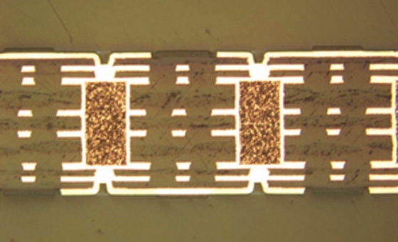
Solder mask, often referred to as solder resist, is a thin protective layer applied to the copper traces of a PCB. Its primary functions are to prevent short circuits, protect against oxidation, and guide solder to the correct areas during assembly. However, if the solder mask isn't applied correctly—whether due to poor coverage or misregistration—it can lead to defects like exposed copper, solder bridges, or unreliable connections. This is where IPC-A-600 comes in, offering clear guidelines to ensure the solder mask meets quality standards.
For engineers and manufacturers, adhering to IPC-A-600 is essential for producing reliable PCBs that meet customer expectations and industry regulations. Whether you're working on consumer electronics or high-reliability applications like aerospace, understanding these standards helps minimize defects and costly rework.
Understanding Solder Mask Coverage Under IPC-A-600
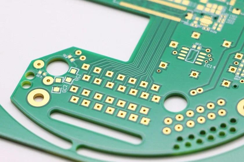
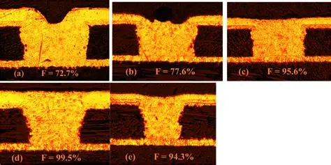
Solder mask coverage refers to how well the protective layer covers the intended areas of the PCB, particularly the copper traces that aren't meant to be soldered. According to IPC-A-600, proper coverage is critical to prevent issues like exposed copper, which can lead to corrosion or unintended electrical connections. The standard defines acceptable and unacceptable conditions for solder mask coverage, providing visual references for inspectors to identify defects.
For instance, IPC-A-600 specifies that the solder mask must fully cover the copper traces in non-soldering areas, with no pinholes, voids, or thin spots that could expose the underlying metal. A common defect is incomplete coverage around vias or pads, where the solder mask might peel back or fail to adhere properly. Such issues are often classified under different acceptability levels—Class 1, 2, or 3—depending on the end-use of the PCB. Class 1 applies to general-purpose electronics with minimal reliability requirements, while Class 3 is for high-reliability applications like medical or military equipment, where even minor defects are unacceptable.
To meet IPC-A-600 solder mask coverage standards, manufacturers must ensure uniform application during the coating process. This often involves using high-quality materials and precise equipment to apply the mask, followed by thorough curing to enhance adhesion. For example, a typical solder mask thickness ranges from 0.8 to 1.2 mils (20 to 30 micrometers), depending on the board design and application. Deviations outside this range could lead to coverage issues, making inspection against IPC-A-600 criteria even more critical.
Related Reading: A Guide to Solder Mask for Beginners
Solder Mask Registration: Precision is Key
Solder mask registration refers to the alignment of the solder mask layer with the underlying copper features of the PCB, such as pads and traces. Misregistration occurs when the solder mask is offset, either covering areas meant for soldering (like pads) or failing to cover areas that need protection. IPC-A-600 provides specific tolerances for solder mask registration, ensuring that the mask aligns accurately with the board's design.
Under IPC-A-600, acceptable registration is defined based on the class of the PCB. For Class 2 boards, often used in industrial or commercial products, a slight misregistration may be tolerable if it doesn't affect functionality. However, for Class 3 boards, the tolerances are much stricter. A common guideline is that the solder mask should not encroach on solderable areas by more than 0.002 inches (0.05 mm) for high-reliability applications. Even a small misalignment can prevent proper soldering or expose critical areas to environmental damage.
Achieving precise solder mask registration requires advanced manufacturing techniques, such as automated optical alignment systems during the mask application process. Additionally, regular calibration of equipment and adherence to design files are crucial to avoid shifts in alignment. For engineers, specifying tight tolerances in the design phase and collaborating closely with manufacturers can help ensure compliance with IPC-A-600 standards for solder mask registration.
PCB Solder Mask Quality: Common Defects and IPC-A-600 Criteria
Ensuring high PCB solder mask quality involves identifying and addressing common defects during inspection. IPC-A-600 categorizes these defects and provides visual aids to help inspectors determine whether a board is acceptable, requires rework, or must be rejected. Let's explore some frequent solder mask issues and how the standard addresses them.
- Pinholes and Voids: Small holes or gaps in the solder mask can expose copper traces, leading to potential short circuits or corrosion. IPC-A-600 specifies that pinholes larger than a certain diameter (often 0.006 inches or 0.15 mm for Class 2) are unacceptable.
- Peeling or Delamination: If the solder mask doesn't adhere properly to the PCB surface, it can peel away over time. The standard requires that the mask remains intact under normal handling and environmental conditions.
- Color and Thickness Variations: Uneven color or thickness can indicate inconsistent application. While minor variations may be acceptable under Class 1, IPC-A-600 demands uniformity for higher classes to ensure reliability.
- Contamination: Dust, oil, or other contaminants trapped under the solder mask can compromise its protective properties. The standard emphasizes clean manufacturing environments to prevent such issues.
By using IPC-A-600 as a benchmark, manufacturers can implement quality control measures to detect these defects early. For example, automated optical inspection (AOI) systems can scan for pinholes or misregistration with high precision, often identifying issues down to 0.001 inches (0.025 mm) in size. Combining such technology with manual inspections ensures that PCB solder mask quality remains consistent across production runs.
Related Reading: Decoding Solder Mask Colors: The Ultimate Guide for PCB Design
Solder Mask Inspection: Best Practices for Compliance with IPC-A-600
Effective solder mask inspection is crucial for ensuring that a PCB meets IPC-A-600 standards. This process involves both visual checks and advanced testing methods to evaluate coverage, registration, and overall quality. Here are some best practices for conducting thorough solder mask inspections:
- Visual Inspection: Start with a detailed visual check under proper lighting and magnification. Inspectors should look for obvious defects like voids, misregistration, or uneven thickness. IPC-A-600 provides detailed images and criteria to guide this process.
- Use of Measurement Tools: Employ precision tools like micrometers or digital microscopes to measure solder mask thickness and registration accuracy. For instance, ensuring the mask doesn't overlap solder pads by more than 0.002 inches (0.05 mm) is critical for Class 3 boards.
- Environmental Testing: Subject the PCB to environmental stress tests, such as thermal cycling or humidity exposure, to verify solder mask adhesion. IPC-A-600 acceptance criteria often include performance under such conditions.
- Automated Systems: Leverage AOI or X-ray inspection systems for detecting hidden defects or inconsistencies. These tools can scan large batches quickly, ensuring no defect goes unnoticed.
- Documentation and Traceability: Maintain detailed records of inspection findings and compare them against IPC-A-600 criteria. This helps in identifying recurring issues and improving manufacturing processes over time.
For manufacturers, training staff on IPC-A-600 standards is a vital step in achieving consistent solder mask inspection results. Certified IPC specialists can provide in-depth knowledge and ensure that every board meets the required class specifications, whether it's for consumer gadgets or critical systems.
How IPC-A-600 Classes Impact Solder Mask Requirements
IPC-A-600 divides PCBs into three classes based on their intended use, and each class has different requirements for solder mask coverage and registration. Understanding these classes helps manufacturers tailor their processes to meet specific quality levels.
- Class 1 – General Electronic Products: These are everyday consumer products like toys or basic appliances. Solder mask requirements are less stringent, allowing minor cosmetic defects as long as functionality isn't affected.
- Class 2 – Dedicated Service Electronic Products: Used in industrial and commercial applications, Class 2 PCBs require better reliability. Solder mask defects like small pinholes may be acceptable if they don't impact performance, but registration must be precise enough to avoid soldering issues.
- Class 3 – High-Reliability Electronic Products: Reserved for critical applications like aerospace or medical devices, Class 3 demands near-perfect solder mask application. Even tiny misalignments (beyond 0.001 inches or 0.025 mm) or coverage gaps are often unacceptable.
Choosing the right class during the design and manufacturing stages ensures that solder mask application aligns with the end-use requirements. For high-stakes projects, investing in tighter controls and advanced inspection methods pays off by preventing failures in the field.
Tips for Achieving Optimal Solder Mask Coverage and Registration
Meeting IPC-A-600 standards for solder mask isn't just about inspection—it's also about optimizing the manufacturing process. Here are some practical tips for engineers and manufacturers to achieve excellent solder mask coverage and registration:
- Design with Tolerances in Mind: Specify clear solder mask tolerances in your PCB design files. For example, ensure a minimum clearance of 0.003 inches (0.075 mm) around solder pads to account for potential misregistration.
- Select Quality Materials: Use high-grade solder mask materials that offer good adhesion and durability. Liquid photoimageable (LPI) solder masks, for instance, provide better precision for complex designs compared to older dry film options.
- Calibrate Equipment Regularly: Ensure that screen printing or coating equipment is calibrated to apply the solder mask evenly, maintaining a consistent thickness of around 0.8 to 1.2 mils (20 to 30 micrometers).
- Control Environmental Factors: Maintain a clean, dust-free manufacturing environment to prevent contamination under the solder mask. Temperature and humidity control during curing also enhances adhesion.
- Collaborate with Your Manufacturer: Work closely with your PCB fabrication partner to align on IPC-A-600 requirements from the start. Regular communication during prototyping can catch potential issues early.
By focusing on these areas, you can significantly reduce the risk of solder mask defects and ensure compliance with industry standards.
Conclusion: Elevating PCB Quality with IPC-A-600 Solder Mask Standards
The IPC-A-600 standard is an invaluable tool for ensuring high-quality solder mask application on PCBs. By defining clear criteria for coverage and registration, it helps manufacturers and engineers produce boards that are both reliable and durable. Whether you're aiming for basic Class 1 compliance or the stringent demands of Class 3, adhering to these guidelines minimizes defects, enhances performance, and boosts customer satisfaction.
From understanding common solder mask defects to implementing rigorous inspection practices, mastering IPC-A-600 standards is a must for anyone in the PCB industry. By prioritizing solder mask quality, you're not just meeting a checklist—you're building trust in every board you produce. At ALLPCB, we're committed to supporting your journey with resources and expertise to achieve excellence in every layer of your PCB design and manufacturing process.