 ALLPCB


In the world of electronics manufacturing, ensuring the reliability of printed circuit boards (PCBs) is critical. One key aspect of this process is ICT testing for solder joints, a method that verifies the connectivity and integrity of soldering points on a PCB. If you're searching for insights on ICT testing, solder joints, and soldering techniques, you've come to the right place. This blog dives deep into how ICT testing ensures flawless connectivity, offering practical information for engineers and manufacturers.
At its core, ICT (In-Circuit Testing) is a powerful testing method used to detect issues in individual components and solder joints on a PCB. By focusing on electrical performance, ICT helps manufacturers catch defects like poor soldering or broken connections before a product reaches the market. Let’s explore this topic in detail, from the basics of ICT testing to best practices for ensuring strong solder joints.
What Is ICT Testing and Why Does It Matter for Solder Joints?
ICT testing, or In-Circuit Testing, is a widely used technique in PCB manufacturing to evaluate the functionality of individual components and connections on a board. Unlike other testing methods that focus on the overall performance of a PCB, ICT zeroes in on specific elements, including solder joints, to ensure they meet electrical standards.
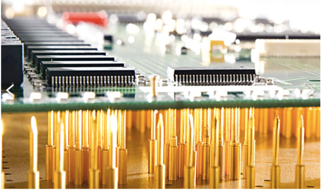
Solder joints are the critical points where components are attached to the PCB. A weak or defective solder joint can lead to poor connectivity, resulting in device failure. ICT testing uses specialized equipment, often called a "bed of nails" fixture, to make direct contact with test points on the PCB. This setup measures parameters like resistance, capacitance, and voltage to confirm that each solder joint is functioning correctly.
Why is this important? A single faulty solder joint can cause an entire circuit to fail. For high-volume production, undetected issues can lead to costly recalls or customer dissatisfaction. ICT testing helps manufacturers achieve near 100% quality assurance by identifying problems early in the production process.
How ICT Testing Evaluates Solder Joints
The process of ICT testing for solder joints is both precise and systematic. Here's a breakdown of how it works:
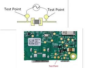
- Test Fixture Setup: A custom fixture with probes is designed to align with the test points on the PCB. These probes make direct contact with solder joints and component leads.
- Electrical Measurements: The ICT equipment sends small electrical signals through the probes to measure parameters like resistance. For example, a typical good solder joint might show a resistance of less than 0.1 ohms, while a defective joint could show a much higher value or an open circuit.
- Defect Detection: ICT can detect issues such as cold solder joints (where the solder hasn’t properly bonded), open circuits (no connection), or shorts (unintended connections between points).
- Data Analysis: The test results are compared against predefined thresholds to determine if the solder joint passes or fails. This data can be logged for quality control purposes.
By focusing on these details, ICT testing ensures that each solder joint provides the necessary connectivity for the circuit to function as intended. For instance, in high-speed digital circuits, even a slight increase in resistance at a solder joint (say, from 0.1 ohms to 1 ohm) can affect signal integrity, leading to data errors.
Common Solder Joint Issues Detected by ICT Testing
Solder joints are prone to a variety of defects, especially in high-volume manufacturing where consistency can be challenging. ICT testing excels at identifying these issues early. Here are some common problems it detects:
- Cold Solder Joints: These occur when the solder doesn’t fully melt during the soldering process, resulting in a weak mechanical and electrical connection. ICT often detects this as high resistance or an intermittent connection.
- Cracked Joints: Physical stress or thermal cycling can cause solder joints to crack over time. ICT can identify these by detecting open circuits or fluctuating resistance values.
- Insufficient Solder: Too little solder can lead to poor connectivity. ICT measurements might show higher-than-expected resistance in such cases.
- Short Circuits: Excess solder or misalignment can create unintended connections between adjacent pads or traces. ICT identifies these as low resistance between points that should be isolated.
Addressing these issues during the manufacturing stage saves time and money compared to dealing with failures in the field. ICT testing provides a reliable way to catch defects before they become bigger problems.

Best Practices for ICT Testing of Solder Joints
To maximize the effectiveness of ICT testing for solder joints, manufacturers must follow certain best practices. These steps ensure accurate results and help maintain high-quality standards in PCB production.
1. Design for Testability (DFT)
Before manufacturing even begins, PCB designs should include test points for ICT probes. These points should be placed near critical solder joints and components to allow easy access during testing. A well-thought-out design can reduce testing time and improve accuracy. For example, test points spaced at least 2.54 mm apart (a common standard) help avoid probe misalignment.
2. Use High-Quality Fixtures
The test fixture is the heart of ICT testing. Investing in a durable, precise fixture ensures consistent contact with solder joints. Poorly designed fixtures can lead to false positives or negatives, wasting time on retesting. Regular maintenance of probes, such as cleaning to remove solder residue, is also essential.
3. Set Accurate Test Parameters
Define clear thresholds for acceptable measurements during ICT testing. For instance, a resistance value above 0.5 ohms might indicate a problem for certain high-current solder joints, while low-current joints might tolerate slightly higher values. Tailor these parameters to the specific requirements of your PCB design.
4. Combine ICT with Other Testing Methods
While ICT is excellent for electrical testing, it may not detect visual defects like uneven solder distribution. Pairing ICT with Automated Optical Inspection (AOI) can provide a more comprehensive quality check. AOI can spot physical flaws, while ICT confirms electrical performance.
5. Regularly Update Test Programs
As PCB designs evolve, so should the ICT test programs. Updating the software to account for new components or layouts ensures that solder joints are tested under the correct conditions. This is especially important for complex boards with high component density.
Benefits of ICT Testing for Solder Joints in PCB Manufacturing
Implementing ICT testing offers several advantages for manufacturers focused on quality and reliability. Here’s why it’s a must-have in modern electronics production:
- Early Defect Detection: Catching issues like poor soldering during production prevents costly failures after assembly. Studies suggest that fixing a defect during manufacturing can be up to 10 times cheaper than addressing it post-shipment.
- Improved Product Reliability: Ensuring strong solder joints leads to longer-lasting devices, which is critical for industries like automotive or medical electronics where failure is not an option.
- High Throughput: ICT testing is fast, often completing a full board check in under a minute for simple designs. This makes it ideal for high-volume production runs.
- Detailed Feedback: ICT provides specific data on each solder joint, helping engineers pinpoint and resolve issues quickly. For example, a resistance reading of 5 ohms on a specific joint can guide targeted rework.
These benefits make ICT testing a cornerstone of quality control in PCB manufacturing, particularly when it comes to ensuring the integrity of solder joints.
Challenges in ICT Testing for Solder Joints
While ICT testing is highly effective, it’s not without challenges. Understanding these hurdles can help manufacturers prepare and adapt their processes accordingly.
- Complex Designs: Modern PCBs often have high component density, making it difficult to place test points for every solder joint. This can limit the scope of ICT testing on some boards.
- Fixture Costs: Custom test fixtures can be expensive, especially for low-volume production. The initial investment might be a barrier for smaller manufacturers.
- False Results: Poor probe contact or outdated test programs can lead to inaccurate readings. For instance, a dirty probe might misread a good solder joint as having high resistance.
To overcome these challenges, manufacturers can invest in flexible testing solutions, such as flying probe testers for low-volume runs, or ensure regular calibration of ICT equipment to maintain accuracy.
Soldering Techniques to Support ICT Testing Success
While ICT testing is a powerful tool for quality assurance, the soldering process itself plays a huge role in the reliability of solder joints. Here are some key soldering practices that complement ICT testing:
- Use the Right Solder Alloy: Choosing a solder alloy with the correct melting point and composition (such as a lead-free SAC305 alloy) ensures strong, consistent joints that pass ICT checks.
- Control Soldering Temperature: Overheating can damage components or create weak joints, while underheating can result in cold solder joints. For most lead-free solders, a reflow temperature of 240-260°C is ideal.
- Ensure Clean Surfaces: Contaminants like flux residue or oxidation on pads can lead to poor soldering. Proper cleaning before soldering reduces the risk of defects detectable by ICT.
- Monitor Solder Paste Application: Using a stencil to apply solder paste evenly prevents issues like insufficient solder or bridging, which ICT can later detect as faults.
By pairing good soldering practices with ICT testing, manufacturers can achieve a higher first-pass yield, meaning fewer boards need rework after testing.
Conclusion: Building Reliable Connections with ICT Testing
ICT testing for solder joints is an indispensable part of modern PCB manufacturing. By focusing on the electrical integrity of soldering points, this method ensures connectivity and prevents failures that could compromise a device’s performance. From detecting cold solder joints to identifying shorts, ICT provides detailed insights that help manufacturers maintain high-quality standards.
For engineers and manufacturers, combining ICT testing with robust soldering techniques and design for testability creates a powerful strategy for success. The result is reliable, long-lasting electronics that meet the demands of today’s fast-paced industries. Whether you’re working on consumer gadgets or critical industrial systems, prioritizing solder joint quality through ICT testing is a step toward excellence in connectivity.
With the right approach, ICT testing not only catches defects but also builds confidence in every PCB that leaves the production line. Embrace these practices to ensure your solder joints—and your products—stand the test of time.


