Calculating the optimal panel size for PCB assembly is a critical step to maximize throughput, improve material utilization, and reduce manufacturing costs. In simple terms, the ideal panel size balances the number of individual PCBs that can fit on a panel with the efficiency of the assembly process and the constraints of manufacturing equipment. To achieve this, you need to consider factors like PCB dimensions, panel dimensions, spacing requirements, and assembly line capabilities. In this comprehensive guide, we'll walk you through the process of determining the best panel size for your project, ensuring high assembly throughput and optimal material utilization.
Why PCB Panel Size Matters for Assembly Throughput and Material Utilization
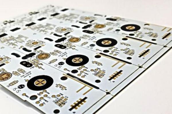
PCB panel size directly impacts how efficiently you can manufacture and assemble printed circuit boards. A panel is a larger board that holds multiple smaller PCBs during production. By arranging multiple PCBs on a single panel—a process called panelization—you can streamline manufacturing, reduce handling time, and minimize material waste. However, if the panel size or layout isn’t optimized, you risk slowing down assembly lines, wasting materials, or even damaging boards during separation.
Optimizing panel size helps achieve:
- Higher Assembly Throughput: More PCBs processed per cycle means faster production.
- Better Material Utilization: Efficient layouts reduce scrap and lower costs.
- Reduced Manufacturing Time: Fewer panel changes and setups speed up the process.
In the following sections, we’ll dive into the step-by-step process of calculating the optimal panel size and explore strategies for manufacturing optimization.
Understanding Key Factors in PCB Panel Size Optimization
Before calculating the optimal panel size, you need to understand the variables that influence panelization. These factors will guide your decisions and help you balance throughput with material efficiency.
1. PCB Dimensions and Shape
The size and shape of your individual PCB are the starting points for panel design. Smaller PCBs allow more units per panel, but irregular shapes can complicate layouts and lead to wasted space. For example, a rectangular PCB measuring 50mm x 30mm will fit more easily into a grid layout than an L-shaped board of the same area.
2. Panel Dimensions and Manufacturer Constraints
Most fabrication and assembly lines have standard panel sizes, often ranging from 18” x 24” (457mm x 610mm) to smaller formats like 9” x 12” (229mm x 305mm). You must work within these limits to ensure compatibility with equipment. Check with your manufacturing partner for their specific panel dimension constraints before starting your design.
3. Spacing and Edge Clearances
Spacing between individual PCBs on a panel, often called “breakaway tabs” or “mouse bites,” is necessary for easy separation after assembly. A typical spacing is 2-3mm, but this varies based on the separation method (routing or scoring). Additionally, most manufacturers require a border clearance of 5-10mm around the panel edges for handling and tooling.
4. Assembly Equipment Capabilities
Your assembly line’s pick-and-place machines, reflow ovens, and testing equipment have limits on the panel sizes they can handle. For instance, a pick-and-place machine might process panels up to 510mm x 460mm at a speed of 50,000 components per hour. Exceeding these dimensions could slow down the assembly throughput or require costly equipment adjustments.
5. Material Utilization Goals
Maximizing the number of PCBs per panel reduces material waste, but over-packing can lead to handling issues or damage during depanelization. Aim for a layout that uses at least 80-90% of the panel area while maintaining safe spacing.
Step-by-Step Guide to Calculate Optimal PCB Panel Size
Now that you understand the influencing factors, let’s walk through the process of calculating the optimal panel size for maximum assembly throughput and material utilization. Follow these steps to create an efficient panel layout.
Step 1: Determine Individual PCB Dimensions
Start by noting the exact dimensions of your PCB. Let’s use an example of a rectangular board that is 60mm long and 40mm wide. If your board has an irregular shape, calculate the smallest rectangle that can enclose it to simplify panelization.
Step 2: Account for Spacing and Clearances
Add the necessary spacing between boards and around the panel edges. Using our example:
- Spacing between boards: 3mm (for breakaway tabs).
- Edge clearance: 10mm on all sides of the panel.
This means each PCB will effectively occupy a space of 63mm x 43mm (including spacing on one side and below) within the panel grid, though you’ll adjust for shared spacing between adjacent boards later.
Step 3: Select a Standard Panel Size
Choose a panel size based on your manufacturer’s capabilities. For this example, let’s assume a common panel size of 300mm x 400mm. After accounting for a 10mm edge clearance on all sides, the usable area becomes 280mm x 380mm.
Step 4: Calculate the Number of PCBs per Panel
Divide the usable panel dimensions by the effective PCB dimensions (including spacing) to determine how many boards fit along each axis.
- Along the length (380mm usable): 380mm ÷ 63mm ≈ 6 boards (rounded down to avoid overlap).
- Along the width (280mm usable): 280mm ÷ 43mm ≈ 6 boards.
This gives a grid of 6 x 6, or 36 PCBs per panel. However, since spacing is shared between adjacent boards, recalculate the actual space used:
- Length: (6 boards x 60mm) + (5 gaps x 3mm) = 360mm + 15mm = 375mm (fits within 380mm).
- Width: (6 boards x 40mm) + (5 gaps x 3mm) = 240mm + 15mm = 255mm (fits within 280mm).
The layout works, with 36 PCBs per panel and minimal wasted space.
Step 5: Evaluate Material Utilization
Calculate the panel area used by the PCBs versus the total usable area to assess efficiency.
- Total PCB area: 36 x (60mm x 40mm) = 86,400mm2.
- Usable panel area: 280mm x 380mm = 106,400mm2.
- Utilization rate: (86,400 ÷ 106,400) x 100 ≈ 81%.
An 81% utilization rate is acceptable, though you might tweak the layout or panel size to push closer to 90% if possible.
Step 6: Assess Assembly Throughput Impact
Finally, consider how this panel size affects assembly speed. If your pick-and-place machine processes one panel every 2 minutes, a 36-PCB panel yields 18 PCBs per minute. Compare this to a smaller panel (e.g., 200mm x 300mm with 16 PCBs) at the same processing time, which yields only 8 PCBs per minute. The larger panel clearly boosts throughput, provided it fits within equipment limits.
Strategies for Manufacturing Optimization with Panelization
Beyond calculating panel size, consider these strategies to further enhance assembly throughput and material utilization.
1. Use Software Tools for Panel Layout
Specialized design software can automate panelization, testing multiple layouts to find the most efficient arrangement. These tools account for spacing, rotation, and irregular shapes, often achieving utilization rates above 90%.
2. Rotate Boards for Better Fit
If your PCB dimensions allow, rotating boards by 90 degrees can sometimes fit more units on a panel. In our earlier example, rotating the 60mm x 40mm board might not help, but for other sizes, this can make a significant difference.
3. Mix Different PCB Designs on One Panel
For low-volume runs or prototypes, combining different PCB designs on the same panel can maximize material use. Ensure the designs have similar manufacturing requirements (e.g., layer count, thickness) to avoid complications.
4. Optimize Depanelization Methods
Choose between routing (using a CNC machine to cut boards apart) and V-scoring (creating grooves for manual separation) based on your panel layout. Routing allows tighter spacing (1-2mm) but takes longer, while V-scoring needs wider gaps (2-3mm) but is faster for high-volume production.
5. Test Panel Size with Small Batches
Before committing to full production, run a small batch with your calculated panel size. Monitor assembly throughput, error rates, and material waste to confirm your design works in practice.
Common Challenges in PCB Panel Size Optimization
While calculating the optimal panel size can boost efficiency, several challenges may arise. Here’s how to address them:
1. Equipment Limitations
If your calculated panel size exceeds equipment capabilities, scale down to a smaller panel or split production across multiple runs. Prioritize throughput over perfect utilization if resizing slows assembly.
2. Irregular PCB Shapes
For non-rectangular boards, use nesting techniques to fit shapes together like puzzle pieces. Software tools can help minimize wasted space.
3. High Component Density Near Edges
Components too close to board edges can get damaged during depanelization. Leave a 5mm buffer zone around PCB edges for safety, even if it slightly reduces utilization.
Conclusion: Achieving Maximum PCB Assembly Throughput with Optimal Panel Size
Calculating the optimal PCB panel size is a powerful way to enhance assembly throughput, improve material utilization, and streamline manufacturing. By carefully considering PCB dimensions, spacing, panel constraints, and equipment capabilities, you can design a panel layout that maximizes efficiency. Use the step-by-step guide provided to determine the best panel size for your project, and apply additional strategies like software tools and layout testing to fine-tune your results.
Whether you’re producing a small batch of prototypes or scaling up for high-volume runs, optimizing panel dimensions is a key step in manufacturing optimization. With the right approach, you’ll save time, reduce costs, and ensure your PCBs are assembled with precision and speed.
 ALLPCB


