ALLPCB


Overview
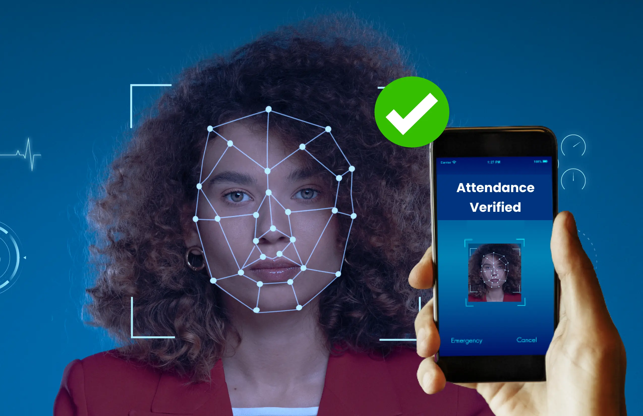
After nearly 10 years of slow organic growth, fingerprint recognition technology is entering a period of rapid development. Experts estimate that over the next five years China will present a market of nearly 10 billion yuan. Fingerprint recognition is currently used mainly for attendance, access control, and safes, and is expected to be applied more widely to identity documents, motor vehicles, and home systems as the technology matures. What are the main techniques for acquiring fingerprint images?
What is fingerprint recognition
Fingerprint recognition leverages the uniqueness and stability of fingerprints and integrates sensors, biotechnology, digital image processing, pattern matching, and electronic engineering.
Development trends
The large market potential for fingerprint recognition will significantly affect the international and Chinese security industries. Smaller companies will face fierce competition from established firms entering the market, and industry consolidation is likely. Over time, traditional industry companies or large investors may come to dominate the biometric recognition sector, although some companies with strong core capabilities may grow rapidly and coexist with larger players. The competitive outcome will likely form a mature industry.
Whether fingerprint products reach large-scale civilian adoption depends on consumer awareness, product stability, and price. Scaled civilian deployment requires three conditions: sufficient consumer awareness, stable product quality with reliable service, and acceptable pricing.
Consumer awareness refers to understanding of fingerprint applications among manufacturers, distributors, system integrators, and end users. For example, when access control requires fingerprint modules, more than 80% of cases are driven by end-user demand, while many access control manufacturers and integrators do not proactively recommend fingerprint products. Low awareness among intermediaries is a major barrier to widespread adoption.
Product stability requires manufacturers to have a thorough understanding of the security industry and to deliver devices that meet usage specifications, customer requirements, and service guarantees.
Price is crucial during product development. Even if a product is stable, it will not be adopted if the price is unacceptable. Positioning in the mid-range and emphasizing terminal-market advantages is a practical approach for civilian markets.
Types of fingerprint acquisition technologies
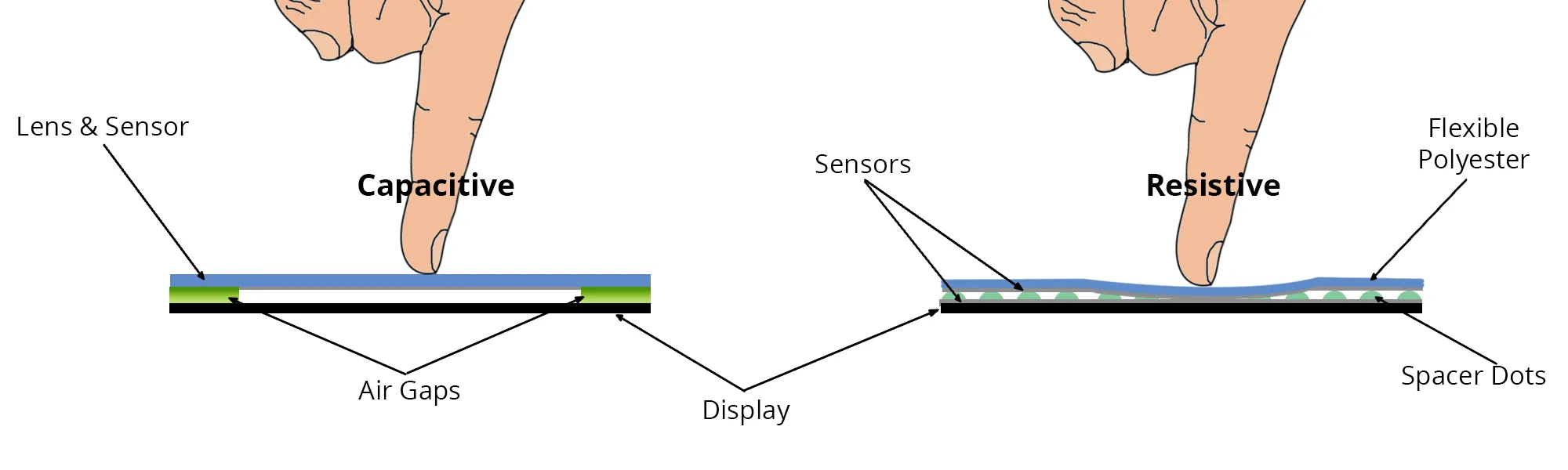
Fingerprint image acquisition techniques mainly include optical scanning devices (for example, miniature prism arrays), thermal differential sensors, semiconductor fingerprint sensors, and ultrasonic fingerprint scanners.
Optical recognition
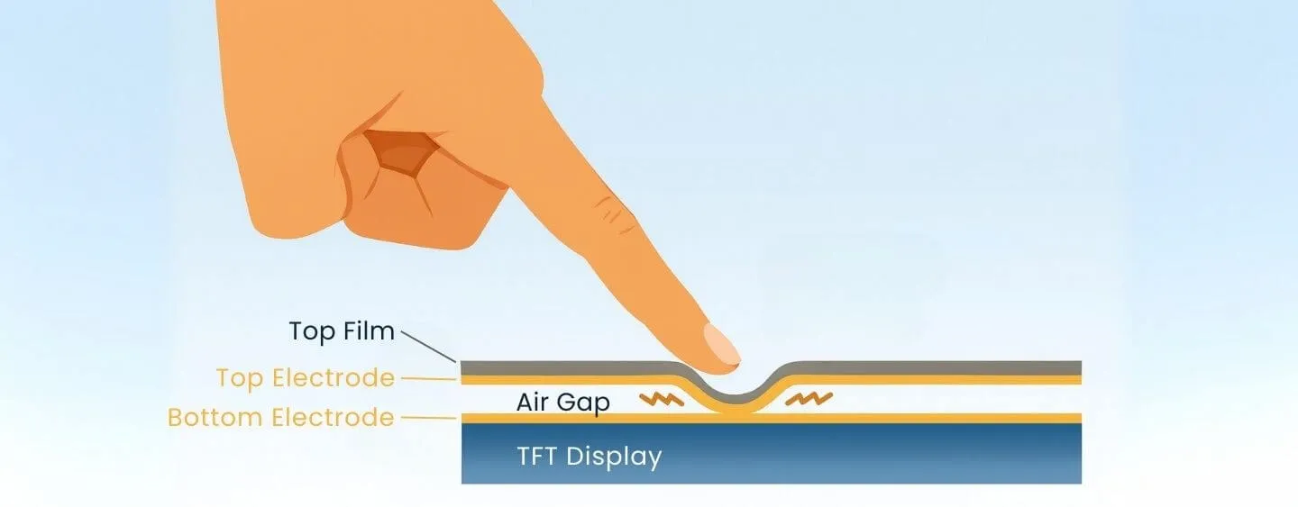
Optical fingerprint acquisition is the oldest and most widely used method. The finger is placed on an optical platen and illuminated; a prism projects the fingerprint onto a charge-coupled device (CCD), producing a grayscale image where ridges appear dark and valleys appear light. The digital image can then be processed by matching algorithms.
Advantages of optical techniques include long track record, tolerance to some temperature variation, and the ability to achieve relatively high resolution (for example, around 500 DPI). The main advantage has historically been low cost. Disadvantages include the requirement for a relatively long optical path, which increases device size, and degraded performance for excessively dry or oily fingers.
Optical systems are limited by latent prints left on the platen after touch; latent prints reduce image quality and can overlap with new prints, complicating practical use. Platen coatings and CCD arrays wear over time, which may degrade image quality. Optical systems also generally cannot perform liveness detection and are sensitive to finger cleanliness, since light cannot penetrate beyond the outer skin layer.
There have been reported incidents of biometric bypass using severed fingers to operate optical readers. In addition, low-cost silicone fingerprint molds available from online marketplaces, sold for around 100 yuan, have been demonstrated to defeat some optical fingerprint readers, enabling fraudulent use such as surrogate attendance punching.
Optical sensors often include prisms with relatively large volumes, typically several times or more the size of semiconductor sensors, limiting optical sensors' use in compact devices. While cost has been a historic optical advantage, the emergence of capacitive semiconductor sensors has narrowed this gap. Many companies still use optical sensors, but the trend favors higher-quality semiconductor capacitive sensors.
Thermal differential sensing
Thermal differential sensors are based on temperature sensing. Each pixel functions like a micro thermal sensor that detects the temperature difference between the finger and a point on the sensor surface, producing an electrical signal that represents image information.
The advantages include fast acquisition, typically within 0.1 s, and very small sensor area; swipe-type fingerprint readers often use this technology. A main drawback is thermal equilibration: over time the finger and the sensor approach the same temperature, degrading contrast.
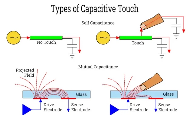
Semiconductor silicon sensing (capacitive)
Since the late 1990s, semiconductor silicon capacitive sensing has matured. The silicon sensor acts as one electrode while the finger acts as the other. Capacitance differences between ridges and valleys relative to the smooth silicon surface produce an 8-bit grayscale image. The electrical signal penetrates the finger surface and the outer nonliving skin layer, reaching the live dermal layer to read fingerprint patterns directly. Because sensing reaches deeper skin layers, the sensor captures more reliable data, is less affected by surface dirt, and improves recognition accuracy.
Semiconductor fingerprint sensors include pressure-based and thermal-based variants, but capacitive sensors are the most widely used.
Capacitive sensors work by precharging sensing elements at each pixel to a reference voltage. When the finger contacts the sensor, differences in distance between ridges and valleys produce different capacitance values. Discharge currents differ accordingly: pixels under ridges (higher capacitance) discharge more slowly, while pixels under valleys (lower capacitance) discharge faster. Measuring discharge rates reveals ridge and valley positions to form the fingerprint image.
Unlike optical systems that often require manual adjustments, capacitive sensors use automatic control to adjust per-pixel sensitivity and local dynamic range. This enables detection of low-contrast areas, such as lightly pressed regions, by increasing sensitivity during capture to generate high-quality images.
Advantages of semiconductor capacitive sensors include superior image quality with minimal distortion, small size, and easy integration into various devices. Because the electronic signal reaches the dermal layer, system security is significantly enhanced.
A key advantage of semiconductor silicon sensing is the ability to perform liveness detection. Capacitive sensors can achieve high image quality on small surfaces, obtaining 200 to 300 lines of resolution on a 1 cm by 1.5 cm area. Their small size, low power consumption, and falling costs make them suitable for security and high-end consumer electronics, and they are often described as the second-generation technology after optical sensors.
Capacitive sensor manufacturing requires complex processes and dense sensing elements per area, involving advanced IC design, large-scale integrated circuit manufacturing, and packaging technologies. As a result, most capacitive sensors are designed and manufactured in regions with advanced IC industries such as the United States, Europe, and others. In China, only a few manufacturers currently have the capability to produce semiconductor fingerprint sensors.
Drawbacks include susceptibility to static interference, which can be mitigated through grounding during installation. While costs were previously high, they have decreased significantly in recent years and are approaching optical sensor costs, making capacitive sensing the current preferred technology for many applications. High-security venues such as bank vaults and correctional facilities can use semiconductor capacitive sensors for front-end liveness detection, replacing passwords, access cards, or optical readers to ensure unique identification.
Ultrasonic technology
Ultrasonic fingerprint acquisition is a newer method that uses ultrasonic waves capable of penetrating materials and producing echoes that vary by material. Because skin and air present different acoustic impedances, ultrasonic reflections can distinguish ridges from valleys. The ultrasonic frequencies used range from about 1×10^4 Hz to 1×10^9 Hz, with energy levels controlled to be safe for the human body, comparable to medical diagnostic intensities.
Ultrasonic systems can achieve very high accuracy and are less sensitive to finger and platen cleanliness. However, acquisition time is typically longer than for optical or capacitive sensors, the devices tend to be expensive, and current implementations are not widely used.