ALLPCB


Overview
HBM4 is under development as the next-generation HBM. HBM (High Bandwidth Memory) is a 3D-stacked DRAM technology that provides high bandwidth, high capacity, low latency, and low power consumption for high-performance computing, artificial intelligence, and data center applications. This article explains HBM principles, advantages, applications, and development trends.
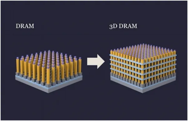
01. HBM Principles: 3D Stacking for High-Density Memory
HBM uses multiple DRAM dies connected via through-silicon vias (TSVs) and micro-bumps (uBumps) to form a stacked memory die. One or more stacks are placed alongside a logic chip (for example, a GPU or CPU) on a silicon interposer. The 3D stacking and short interconnects enable much higher capacity and substantially wider interfaces compared with conventional memory.
For example, the first-generation HBM (HBM1) stacks four 8 Gb DRAM dies into a 32 Gb stack with a 1024-bit interface per stack. Up to four stacks can be used to reach 128 Gb total capacity and a 4096-bit total interface width. By contrast, a typical DDR4 interface is 64 bits wide, and a single DDR4 chip may be up to 16 Gb; two such chips yield 32 Gb total capacity with a 128-bit total interface width.
02. HBM Advantages: High Bandwidth, Low Latency, Low Power
By enabling high-density 3D stacks with very wide interfaces and short interconnects, HBM delivers three main advantages: high bandwidth, low latency, and low power.
High bandwidth: HBM increases the number of stacks and the interface width per stack, and supports high per-pin data rates. For example, third-generation HBM (HBM3) can support eight stacks with a 2048-bit interface per stack and per-pin rates up to 9.6 Gbps, yielding up to about 1.2 TB/s aggregate bandwidth. By comparison, conventional DDR4 solutions typically offer aggregate bandwidth on the order of tens of GB/s (for example, roughly 64 GB/s for some configurations).
Low latency: HBM reduces the physical distance between memory and logic by placing stacks on an interposer close to the processor and supports parallel access across many independent channels. HBM3 implementations can reduce the memory-to-logic distance to roughly 100 micrometers and provide simultaneous access to multiple independent channels (for example, 16), lowering access latency compared with DDR4, which connects memory across circuit-board traces that can be centimeters long and often serializes channel access.
Low power: HBM lowers operating voltage and reduces the number and length of signal traces, cutting power consumption. HBM3 may operate near 0.7 V and use on the order of several thousand signal lines (for example, about 5,000), while DDR4 typically operates around 1.2 V and requires substantially more signal routing (for example, on the order of 20,000 lines in comparable system implementations), increasing power dissipation.
03. Applications: HPC, AI, and Data Centers
Because of its high bandwidth, low latency, and energy efficiency, HBM is widely used in high-performance computing (HPC), artificial intelligence (AI), and data center systems.
High-performance computing: HPC systems require large capacity, high bandwidth, and low-latency memory to support massive parallel processing. HBM meets these requirements and is used in accelerator products such as NVIDIA's H100 and H800 and AMD's MI300 series, which adopt HBM3 to support demanding HPC workloads.
Artificial intelligence: AI workloads such as large neural network training and inference demand high bandwidth and low-latency memory. HBM is used in AI accelerators; for example, Google reports using HBM2E in its TPU v4 and TPU v5 series.
Data centers: Data center processors and accelerators benefit from HBM's combination of capacity, bandwidth, and energy efficiency. Intel's Sapphire Rapids and Granite Rapids server processors have been reported to use HBM2E in certain configurations to address high-throughput data-center workloads.
04. Development Trends: Vendors and Next-Generation HBM
Major memory vendors are advancing HBM generations to improve performance and capacity.
SK Hynix: SK Hynix announced HBM3 production ramp and has supplied samples to customers including NVIDIA and AMD. SK Hynix's HBM3 supports eight stacks, a 2048-bit interface per stack, and per-pin rates up to 9.6 Gbps, enabling roughly 1.2 TB/s aggregate bandwidth; the company positions HBM3 for HPC, AI, and data-center applications.
Samsung: Samsung announced production of high-performance HBM2E and has supplied samples to customers including Google and Intel. Samsung's HBM2E supports eight stacks, a 1024-bit interface per stack, and per-pin rates up to 4.8 Gbps, delivering about 614.4 GB/s aggregate bandwidth; Samsung positions HBM2E for high-capacity data processing and storage needs.
Micron: Micron reported development plans for HBM4 and targeted production timelines in the 2024 timeframe. Micron's HBM4 is described as supporting up to 16 stacks, a 4096-bit interface per stack, and per-pin rates up to 12 Gbps, potentially enabling up to about 3 TB/s aggregate bandwidth.
Market research firm TrendForce projected significant growth in HBM demand, estimating a year-over-year increase of about 58% in 2023 and further growth in 2024. HBM is expected to remain an important memory technology for high-performance computing, AI, and data-center systems.