ALLPCB


In embedded systems, when two microcontrollers powered at different voltages need to communicate, or when a microcontroller communicates with peripheral devices at different voltages, level translation is required to avoid communication failure or damage to the microcontroller from overvoltage. The following describes five common level translation methods.
1. Resistor divider
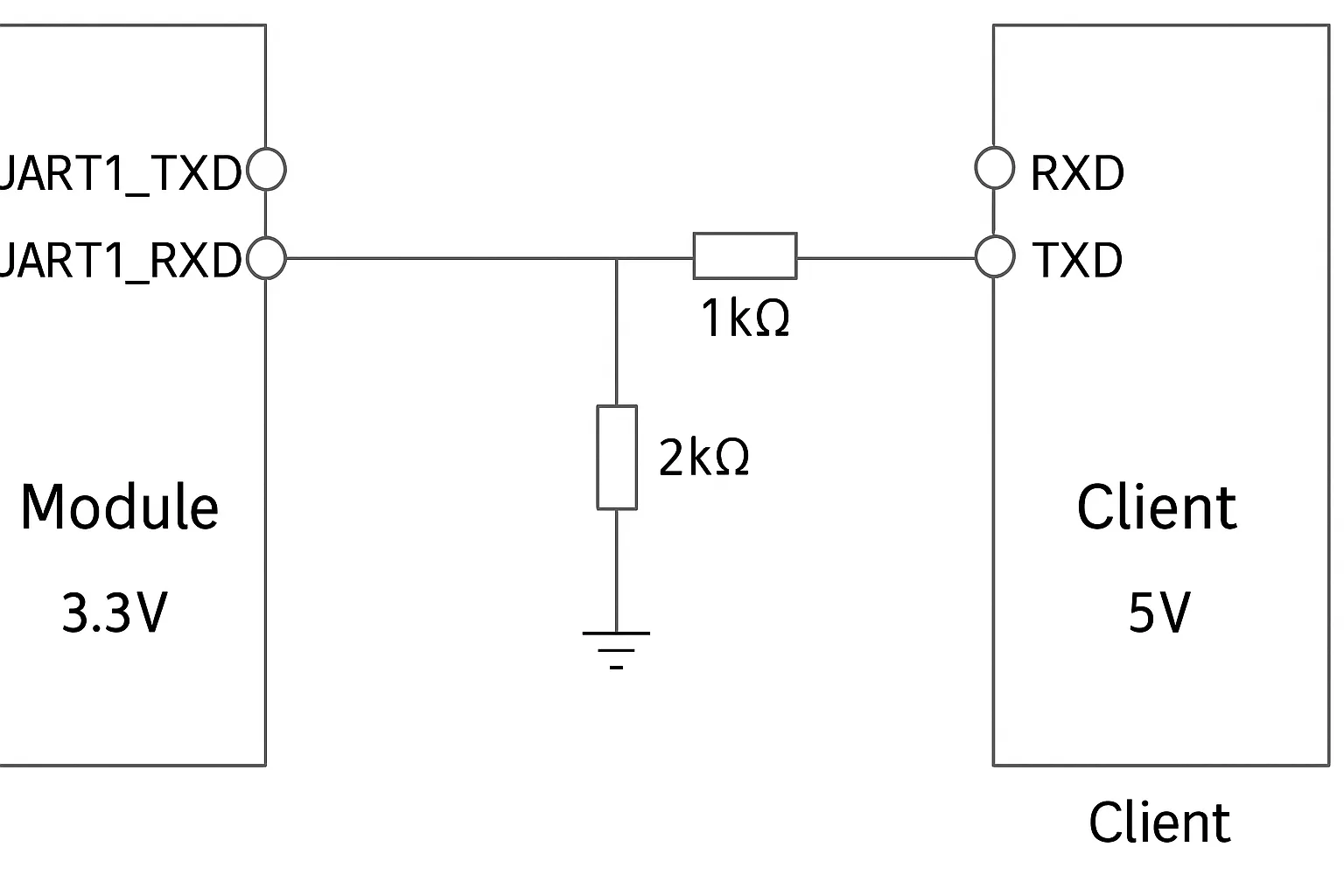
As shown, the left side is a 3.3V system and the right side is a 5V system. When the 5V device transmits toward the 3.3V side, the voltage is divided by two resistors. The receiving voltage is about 5V*2k/(1k+2k) ≈ 3.3V, achieving level matching.
Because only resistors are used, the main advantages are very low cost and simple layout. The disadvantages are relatively high power consumption, limited drive capability, and restricted speed. This approach is generally suitable for frequencies up to about 100 kHz.
2. Level translation ICs
Dedicated level translation ICs perform the conversion internally when supplied with the appropriate voltages on both sides. Examples include the 74xHC and 74xHCT families, which can implement multiple channels of 3.3V-to-5V and 5V-to-3.3V translation.
Using an IC provides strong drive capability (CMOS outputs), low leakage current, suitability for multiple channels, and high speed. The primary drawback is higher cost.
3. Diode clamp
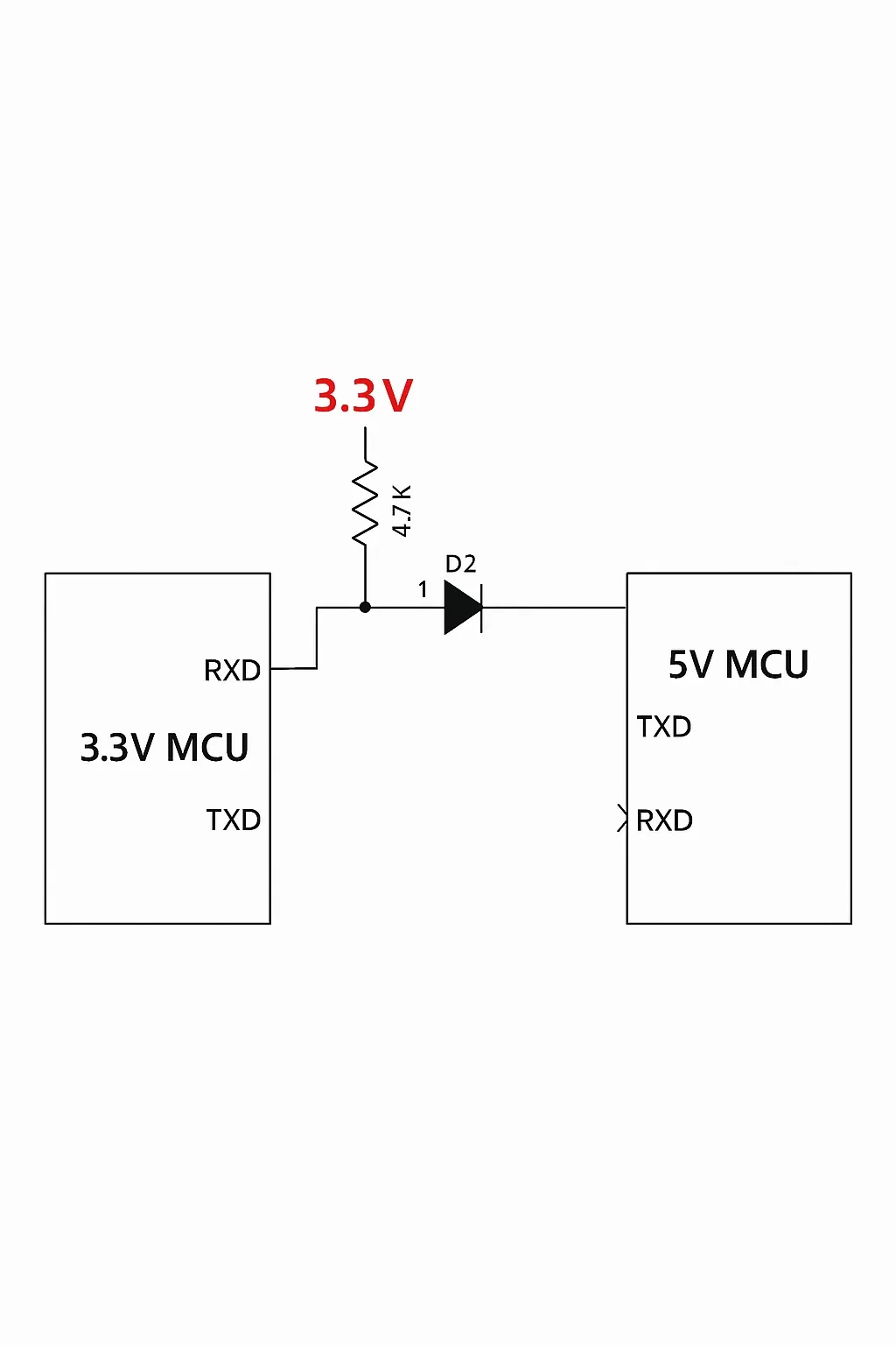
A diode's forward drop can be used for clamping to perform level translation. In the example, when the 5V transmitter on the right outputs a high level, diode D2 is off and the left RX receives a high level of about 3.3V via a pull-up resistor. When the right transmitter is low, the diode clamps the left RX to about 0.3V, recognized as low. This circuit requires D2 to have a very small forward drop (<0.5V), so Schottky diodes are typically used; otherwise the levels may not match reliably.
The diode clamp method offers low leakage and low cost. Its disadvantages include strict diode drop requirements, limited drive capability, and lower transmission speed.
4. Bipolar transistor
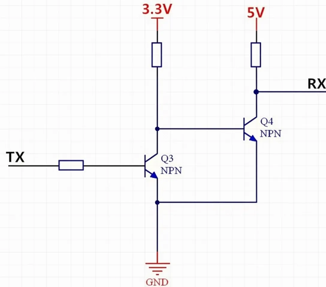
The circuit shown uses two NPN transistors to convert a 3.3V input signal to a 5V output while maintaining signal synchronization. When TX is low, Q3 is off, Q4 conducts, and RX is pulled to ground. When TX is high, Q3 conducts, Q4 is off, and RX is pulled up to 5V. This keeps the two sides synchronized and translates the level.
Advantages include low cost, strong drive capability, and a mature, widely used circuit. Disadvantages are waveform delay introduced by the transistors, limiting maximum speed (practical baud rate not to exceed 230400). Multiple-channel implementations require more components and PCB area.
5. MOSFET (bidirectional) for I2C
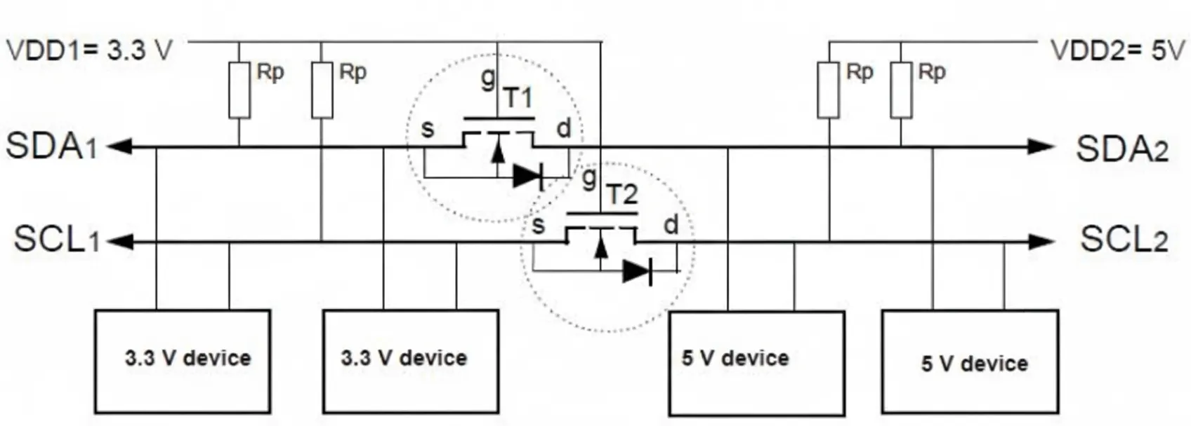
The diagram shows the classic MOSFET-based bidirectional level shifter used for I2C between 5V and 3.3V. When SDA1 is high, the MOSFET has no VGS so it is off, and SDA1 and SDA2 both remain high but at their respective voltages. When SDA1 is low, the MOSFET conducts and both SDA1 and SDA2 are low. SCL behaves similarly.
This method is suitable for low-frequency signals, is inexpensive, has lower voltage drop than bipolar transistors, and typically supports speeds up to about 400 kHz.