Introduction
This summary is based on practical EMC design work in military projects, trainings on electronic countermeasures, participation in EMC training courses, experience in laboratory EMC remediation, relevant IEEE publications, and exchanges with peers, combined with company test results. It provides practical guidance for the electromagnetic compatibility design of printed circuit boards.
Note: The following provides basic conclusions only. It does not cover detailed topics such as trace length calculations for specific signal frequencies, harmonics and wavelengths, board-level shielding, shield cavity design, aperture sizing and count, cable entry and exit treatments, waveguide cutoff diameter and length calculations, electrostatic protection, or lightning protection. Some conclusions may be incomplete or require correction.
1. Component Layout
EMC-conscious printed circuit board layout should be coordinated among PCB engineers, mechanical designers, and EMC engineers. Balance functional partitioning, thermal distribution, and EMC considerations when placing components.
Key layout considerations:
- Partition by signal speed. Place high-speed devices (fast logic, clock oscillators) near connectors to reduce antenna effects. Place low-speed logic and memory away from connector areas to reduce common-impedance coupling, radiation, and crosstalk.
- On single- or double-sided boards, if power traces are long, add decoupling capacitors to ground every 3000 mil. Typical values: 10 uF and 1000 pF in parallel to filter high-frequency noise on the power rail.
- On single- and double-sided boards, route power through filter capacitors before the IC supply pins so the supply to the IC is filtered. Place decoupling capacitors to minimize ground impedance; their optimal location depends on the specific layout and should minimize return loop area.
- Keep strong radiators such as clock lines, buses, and RF lines at least 1000 mil away from external connector traces to avoid coupling to outgoing signals. Place crystals, oscillators, relays, and switch-mode power supplies with EMC considerations in mind.
- The input and output traces of filters must not run parallel or cross each other in a way that allows direct noise coupling between pre- and post-filter sections.
- Series termination resistors for source matching should be placed close to the driving source.
- Place decoupling capacitors as close as possible to the IC supply pins to reduce high-frequency return loop area and radiation.
- Filter, protection, and isolation components for interfaces should be placed close to the connector and follow the principle "protect first, then filter."
- Place the input filter for the board power supply near the power entry connector.
- When using isolated filter designs for an interface, place RC/LC components as required and ensure the isolation area on other layers contains no unrelated traces.
- Do not place components within 4 mm of the PCB edge.
- Arrange functional blocks following signal flow so traces are short and avoid unnecessary loops.
- Place each function's core component at the center of its block and arrange surrounding components compactly to minimize interconnect length.
- For high-frequency circuits, consider distributed parameters between components; align component orientation where possible.
- Keep sensitive components separated; place input and output elements apart to reduce mutual interference.
- Group components by supply voltage, digital versus analog, speed, and current to avoid mutual interference. Arrange connector pin assignments accordingly. Place all connectors on one board edge when possible to reduce common-mode radiation from cables.
- Place a high-frequency bypass capacitor near each IC supply pin; ideally one small high-frequency capacitor per power pin.
- Place energy storage capacitors and high-frequency bypass capacitors near units that have large current transients, such as power modules, fans, and relays.
2. PCB Routing
When routing the board, first finalize component placement, then route ground and power, then high-speed signals, and finally low-speed signals. Route the ground first; ground should form a mesh where practical.
- Power traces: route power traces close to ground to reduce differential-mode loop area and to reduce crosstalk.
- Clock, signal, and ground placement: keep signal traces close to ground to minimize loop area. Where possible, surround clock traces with ground traces or planes and stitch with multiple ground vias to reduce ground impedance and prevent the ground from acting as an antenna.
- Avoid layer transitions for clock and critical signals; if a via is required, place ground vias near the via.
- Keep critical traces such as clock, bus, and RF traces separated from parallel traces on the same layer; follow the 3W rule where applicable.
- Avoid discontinuities: do not change trace width abruptly; avoid sharp corners. Avoid stubs and inconsistent widths.
- Avoid long adjacent parallel runs of input and output traces to reduce crosstalk, except for differential pairs.
- Do not route unrelated signals beneath filters.
- Keep crystal traces close to the IC and surround clock traces with ground. Place clock ground pin and CPU ground pin on the same layer and close to each other to reduce crystal ground loop. Minimum trace widths: clock trace ≥ 10 mil, surrounding ground traces ≥ 20 mil. Expose ground copper under the crystal where appropriate to increase capacitive coupling.
- Route critical signals close to a reference ground plane to minimize return loop area and radiation.
- Keep high-speed traces away from clock/crystal traces; if parallel routing is unavoidable, separate with ground traces.
- Keep critical traces at least 3H away from the edge of their reference plane, where H is the height between the trace and the reference plane, especially for power traces.
- Route analog high and low level signal traces on separate sides of the ground or power plane.
- Differential pairs: route on the same layer, equal length, parallel, and with consistent impedance. Do not route other signals between the pair. If vias are necessary, use paired vias and keep them close.
- Avoid routing critical signals across partitions; if necessary, provide bridging to maintain a continuous return path.
- Minimize return loop area as the primary routing objective.
- Inset power planes relative to adjacent ground planes by 20H where possible, and at a minimum by 5H when constrained by mechanical structure.
- Avoid routing signal and address traces that create ground combs or ducts.
3. Power System EMC Design
Power-related EMC design covers switch-mode power supplies and power delivery for both digital and analog circuits. SMPS EMC design includes front-end common-mode and differential-mode filters, snubber and damping networks for transformers, clamp and snubber for switching devices and fast diodes, and transformer shielding, all tailored to the specific product.
Power delivery for analog and digital circuits requires selection and placement of bulk decoupling capacitors, IC decoupling capacitors, board-level decoupling, ferrite beads, and appropriate filtering topologies.
Switching and rectification loops carry high-amplitude trapezoidal currents with significant harmonic content extending well above the switching fundamental. Peak amplitudes can reach up to five times steady-state DC current and have fast edges (typically ~50 ns). These loops are primary EMI sources and should be routed to minimize loop area. The three main components in each loop—filter capacitors, switching/rectifying devices, and inductors or transformers—should be placed adjacent to each other.
SMPS routing rules:
- Keep all AC-carrying traces short and wide.
- Minimize loop areas to suppress SMPS radiated emissions.
- Use wider traces for higher currents to reduce loop resistance.
- Route power and ground traces following current direction to increase noise immunity.
SMPS grounding rules:
- Single-point grounding is common: the common node of input filter capacitors should be the single connection to the high-current AC return. Place same-stage ground connections close together; stage filter capacitors should connect to the stage ground point to control return currents.
- Use wide ground traces or copper pours for low impedance. If possible, use ground widths ≥ 3 mm or large copper areas; tie unused board areas to ground.
- Control chip grounding: power ground and signal ground should ultimately form a single ground, but power ground and signal ground should form controlled return paths. Do not mix power and signal grounds indiscriminately; connect control ground to main power ground at a single designated point to avoid injecting noise into sensing and amplifier inputs.
4. EMC Design for Digital Circuits
Digital EMC design includes component selection, clock circuit EMC, data and address bus routing, impedance matching, ground bounce mitigation, and filtering at bus drivers.
Prefer devices with slower, smoother edges where performance allows. Fast edges on high-speed logic often produce ringing and harmonic emissions; common mitigations are series damping resistors or ferrite beads on high-speed data lines.
About 90% of EMI typically originates from 10% of critical circuits. Prioritize routing and protection for critical nets such as clocks, high-speed data buses, address buses, reset lines, and control lines.
Grounding for high-speed data circuits generally uses multiple return points to reduce impedance.
Power design for high-speed data circuits:
- Board power entry decoupling typically includes a large electrolytic or bulk capacitor plus one or two small high-frequency bypass capacitors to supply transient charge and filter high-frequency noise.
- Device decoupling: any clocked device should have high-speed bypass capacitors on its supply pins; multiple supply or ground pins must each be decoupled.
Routing rules for high-speed data:
- Keep signal traces close to ground to minimize loop area. Surround clock traces with ground where possible and stitch with ground vias to reduce ground impedance.
- Partition by logic speed: place high-speed devices and clock sources near connectors; place low-speed logic and memory away from connector areas to reduce antenna effects and common-impedance coupling.
- Avoid trace discontinuities: do not change trace width abruptly or use sudden bends.
- Keep I/O traces away from clocks and power traces and avoid placing them adjacent to sensitive lines such as reset, interrupt, or control lines. Reduce long adjacent parallel runs except for differential pairs.
- Avoid stubs, acute angles, and inconsistent widths.
- Keep crystal traces close to the IC and guard them with ground. Place clock ground and CPU ground pins on the same layer and adjacent to reduce crystal ground loop. Minimum widths: clock trace ≥ 10 mil, guard ground ≥ 20 mil.
- Route critical signals near a ground plane to reduce return area and radiation.
- Keep high-speed traces away from clock/crystal traces; if parallel routing is unavoidable, separate with ground.
- Avoid layer change for clock and critical signals; if a via is required, provide ground vias nearby.
- Differential pairs must be routed on the same layer, equal length, parallel, with consistent impedance and no signals between the pair.
- Avoid routing critical signals across partitions; if necessary, provide bridging to maintain a continuous return path.
- For components with metal housings such as crystals, provide ground copper on the top layer under their projected area to create distributed capacitance between the metal housing and ground, reducing emissions and improving immunity.
5. EMC Design for Analog Circuits
Analog EMC design mainly addresses EMS because analog circuits are highly sensitive to interference. Protect analog input ports with appropriate protection devices such as filters, ferrite beads, transient suppressor diodes, common-mode chokes, and isolation transformers.
Analog circuits operate at low frequencies and can be affected by millivolt-level disturbances. For sensitive analog sections, single-point grounding is often preferred to prevent large ground currents from digital circuits, switch-mode supplies, or relays from using the analog ground. Avoid ground loops near sensitive low-frequency analog circuits.
For mixed-signal ICs that contain both analog and digital sections, separate ground planes are not always practical. Often the best approach is a combined ground with careful layout: cluster analog peripheral components together and keep them away from noisy sources.
6. Interface Circuit EMC Design
Interface EMC design includes filtering and protection for connectors and cable interfaces. Filtering reduces radiated and conducted emissions via interfaces and suppresses external interference. Protection ensures circuits withstand overvoltage and overcurrent transients.
Basic design principles for interface filtering and protection:
- Ensure filtering and protection do not unacceptably degrade signal integrity.
- Design filtering and protection based on actual needs; do not copy circuits blindly.
- When both protection and filtering are needed, implement protection first, then filtering.
- Place interface ICs and their filtering, protection, and isolation components in a straight line along the signal flow at the connector.
- Place filter, protection, and isolation components as close to the connector as possible and keep signal connection lengths as short as practicable.
- Place interface transformers close to the connector, typically within 3 cm of the corresponding connector.
- Separate analog and digital interfaces, and separate low-speed and high-speed interfaces by distance according to their sensitivity and emission potential; apply isolation or shielding where connectors may interfere.
- For mixed-signal connectors, use grounded pins to separate different signal types, especially sensitive signals.
- Maintain consistent trace width for interface traces. For high-speed traces, use smooth circular arcs where bends are necessary.
- Do not route other signals between differential pairs or their return traces. Differential pair segments should be parallel, adjacent, and on the same layer, with matched lengths.
- If an interface trace from driver/receiver to the connector exceeds about 2.5 cm, treat it as a transmission line and design for the specified characteristic impedance.
- Avoid routing interface signals across planes unless they pass through an isolation filter.
- Use shielded connectors for many interface types, especially high-frequency interfaces.
- Ensure connector shells have good electrical continuity to the chassis. For connectors that offer 360° mating, ensure full circumferential contact with low contact resistance, typically less than 1 mΩ when specified.
- For connectors that cannot achieve full circumferential contact, use spring tines around the shell with adequate size and spring force to maintain good electrical contact with the chassis.
- Filtered connectors can substantially improve EMC performance but increase cost. Use them where board-level filtering and cable shielding cannot meet requirements.
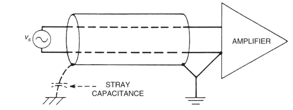
- Ensure cable shield termination to connector shells is as close to 360° as practical to provide low impedance connection to the chassis.
- Where shield termination to the chassis is not feasible, apply equivalent measures to maintain interface EMC performance.
- Follow vendor and standards guidance for impedance matching, filtering, isolation, and protection on interface signals.
7. Mechanical and Enclosure EMC Design
Mechanical EMC design covers backplanes, enclosures, and internal cable routing. Metal enclosures or plastic enclosures with internal metal coating are the most effective way to shield functional units or devices.
Minimize gaps and discontinuities in enclosure seams to control leakage. Improve seam shielding by increasing seam depth, reducing seam length, adding conductive gaskets, applying conductive coatings, and reducing fastener spacing.
Align enclosure openings with magnetic field lines where possible. Openings perpendicular to the magnetic field can increase magnetic reluctance and reduce shielding effectiveness.
Disorderly internal wiring undermines the effectiveness of shielding, filtering, and grounding measures. Proper internal wiring reduces mutual interference between high- and low-level signals and facilitates later remediation.
Basic rules for internal wiring:
- Keep exposed internal wiring as short as possible.
- Bundle and separate wires by signal type. Group digital and analog wiring separately and maintain spacing between bundles.
- For flat ribbon cables used for signals, consider arranging conductors as ground-signal-ground-signal-ground to suppress interference.
- Twist low-frequency forward and return conductors to form twisted pairs, reducing electromagnetic interference.
- Apply shielding to identified high-radiation conductors.
- Ensure shielded cable shields have reliable mating to the enclosure, preferably 360° contact with low contact impedance.
- Unshielded cables should not ideally exit a shielded enclosure directly. If allowed under special conditions, the unshielded portion inside or outside the enclosure should not exceed 80 mm; this length includes board routing between the filter and the enclosure.
- One mitigation for unshielded cables is to apply a metal mesh wrap to the cable inside the enclosure to create a locally shielded section; be aware of manufacturing and effectiveness limitations.
- Some systems require cable shields not be tied to the enclosure on one side, for example certain coaxial installations. In such cases treat the cable as unshielded with the same 80 mm constraint, or use double-shielded cable.
8. Grounding Design
Grounding must provide a low-impedance path. Use wide, short ground conductors and large copper areas on the PCB. Ground loop issues are important at low frequencies; a low-impedance grounding strategy is commonly used to mitigate them.
In high-speed designs, controlling ground impedance is typically more important than eliminating loop topology. Digital circuits often use multipoint grounding to reduce ground impedance. Low-frequency analog and small-signal circuits benefit from single-point grounding to avoid ground loops.
Modern ICs often combine analog and digital functions. A hybrid approach that mixes single-point and multipoint grounding is frequently used: digital sections may use multipoint or large-area ground, while analog sections use single-point grounding.
Implement grounding strategies on the PCB level; system-level grounding becomes more complex when considering signal integrity, EMS, safety, and EMC requirements.
Single-point versus multipoint grounding:
- Single-point grounding suits low-level analog and sensitive circuits because it controls current paths and avoids ground loops.
- Multipoint grounding suits high-frequency circuits because inductance and parasitic capacitance make single-point grounding impractical, increasing ground impedance and creating unintended loop paths.
In practice, separate digital and analog grounds where feasible but tie them at a controlled point. For mixed systems, combine grounds carefully, cluster analog peripherals, and separate noisy sources. Proper implementation can resolve severe hum or noise problems that arise from long cable runs or poor grounding practices.
 ALLPCB


