ALLPCB


A product failed EMC conducted emission tests during network access testing. The DC power port (DC port) showed severe conducted emission exceedance in the low-frequency range from 150 kHz to 2 MHz, with some spectral lines exceeding limits by more than 10 dBμV. After on-site modification of the power boards, the DC port conducted emissions passed retest with margins greater than 5 dBμV.
1. Problem Description
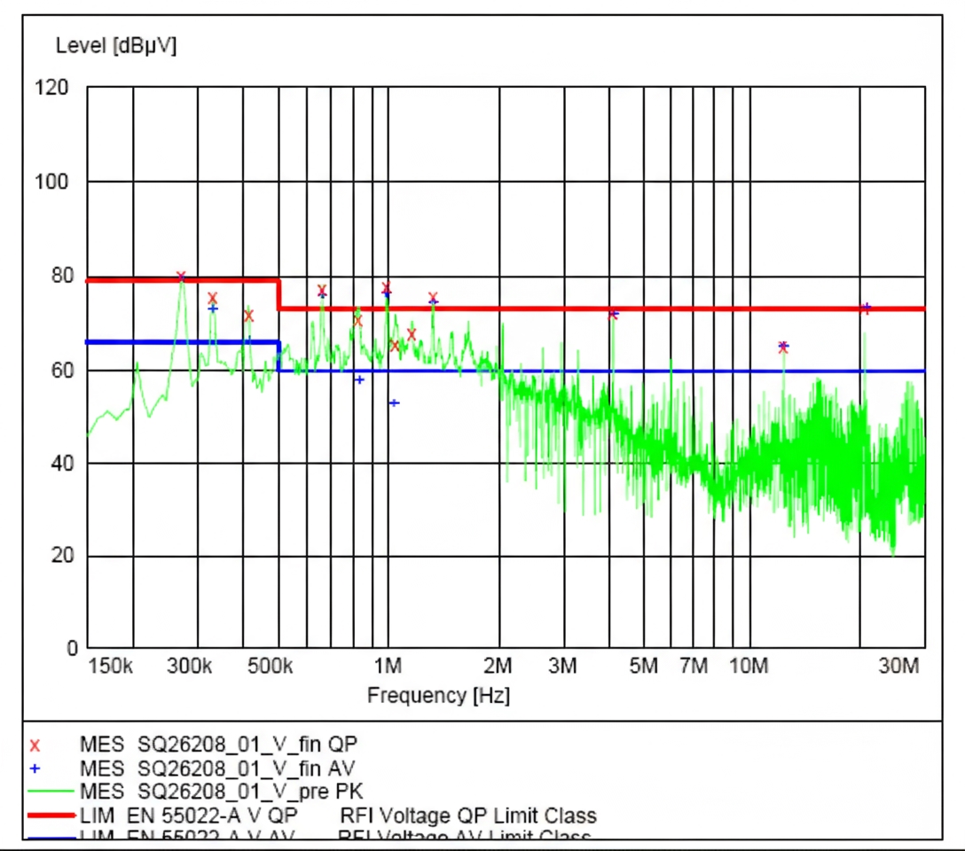
During network access EMC testing, the product's DC power port exhibited conducted emission failures in the 150 kHz to 2 MHz band, with certain frequencies exceeding limits by over 10 dBμV. Test results are shown in Figure 1.
2. Analysis
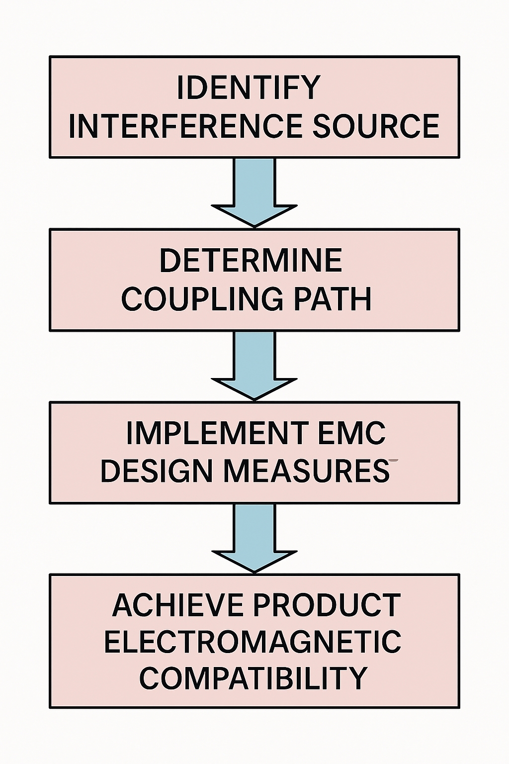
Conducted emissions are among the more challenging EMC items because they measure the electromagnetic disturbance generated by the product itself. To resolve emission issues, first identify the disturbance source and the coupling path. Then apply appropriate EMC design measures based on the source characteristics and coupling mechanism, such as grounding design, filtering, and isolation, to achieve electromagnetic compatibility.
In this case, both the disturbance source and the coupling path were clear. Internal tests at the company replicated the on-site configuration and confirmed the disturbance originated from the system DC power circuitry, including the system power board and the main control board switching power supplies. The coupling path was the -48V and -48VRTN power lines, and the coupling mechanism was conducted coupling. Therefore the focus was on applying appropriate EMC design measures on-site, such as grounding and filtering.
3. Fix Implemented
Photographs from the test site showed the DC power cable present during testing was a 2-conductor cable: blue (-48V) and black (-48VRTN). However, the product is designed to use a 3-conductor power cable: the blue and black power conductors plus a second black conductor for the system working ground GNDD. In normal operation, GNDD should converge with -48VRTN and the cabinet protective ground GNDP inside the cabinet, and then connect to the equipment room ground bus, forming a combined grounding scheme implementing DC-C (Connected) grounding.
Because the test site could not provide a 3-conductor power cable, GNDD was not available at the board-to-cable interface. The requirement was to modify the power board so GNDD would be tied to -48VRTN inside the board, creating a common ground. The modification was implemented by shorting GNDD to -48VRTN with a wire inside the board.
After tying system working ground GNDD to -48VRTN, the combined node was connected to the cabinet protective ground GNDP, forming a single combined ground plane (GNDD, -48VRTN, and GNDP commoned). This composite grounding implements the DC-C grounding approach. The purpose of combining the three grounds is twofold: first, to establish equipotential planes to avoid large potential differences between planes, between plane and signal, or between signals during surges or local high voltages, which could damage board components; second, to provide the lowest-impedance return path for the system. The DC port conducted emission results after the three-ground commoning are shown in Figure 4. Compared with the initial test (Figure 1), the noise decreased generally by more than 10 dBμV, and at some frequencies by as much as 20–30 dBμV, demonstrating the significant impact of three-ground commoning on DC power conducted disturbances.

4. Summary
The final retest showed the modification was highly effective. Compared with the initial results, DC port noise decreased significantly across low and high frequency bands, with some frequencies falling by more than 30 dBμV. Grounding design plays an important role in improving a system's EMC performance, as demonstrated by this case.
Two lessons from this case for similar issues:
- Every electromagnetic disturbance has a source and a coupling path. To solve the problem, first determine the disturbance source. Large signal sources in a circuit often include power supplies, clock circuits, fans, relays, inductive loads, and high-speed ICs. After identifying the source, determine the coupling path: conducted or radiated, common-ground or space coupling, etc. Only after identifying both source and coupling path can effective EMC measures be chosen, such as grounding, filtering, shielding, or isolation.
- There are typically two system grounding approaches: DC-I (Isolated) and DC-C (Connected). Which approach to use depends on the original design and actual deployment. In this case, a DC-C composite grounding approach was required.