 ALLPCB


Embedding components within printed circuit boards (PCBs) is a cutting-edge approach to designing compact, high-performance electronics. If you're searching for PCB design guidelines, embedded component design rules, or tips on design for manufacturability (DFM), you're in the right place. This blog post will guide you through the best practices for PCB layout with embedded components and offer actionable advice, including insights on Altium embedded component design. We'll cover everything from the basics of embedding to advanced strategies for ensuring manufacturability and reliability.
What Is Embedded Component Design in PCBs?
Embedded component design refers to the process of integrating passive or active components, such as resistors, capacitors, or even small ICs, directly into the layers of a PCB. Unlike traditional surface-mount or through-hole techniques, embedding reduces the board's surface area, minimizes signal interference, and enhances reliability by protecting components from environmental factors. This technique is especially valuable in industries like aerospace, automotive, and wearable technology, where space and performance are critical.
By following specific embedded component design rules, engineers can create smaller, more efficient designs while adhering to design for manufacturability (DFM) principles. In the sections below, we'll dive into the detailed steps and best practices to help you master this innovative approach.
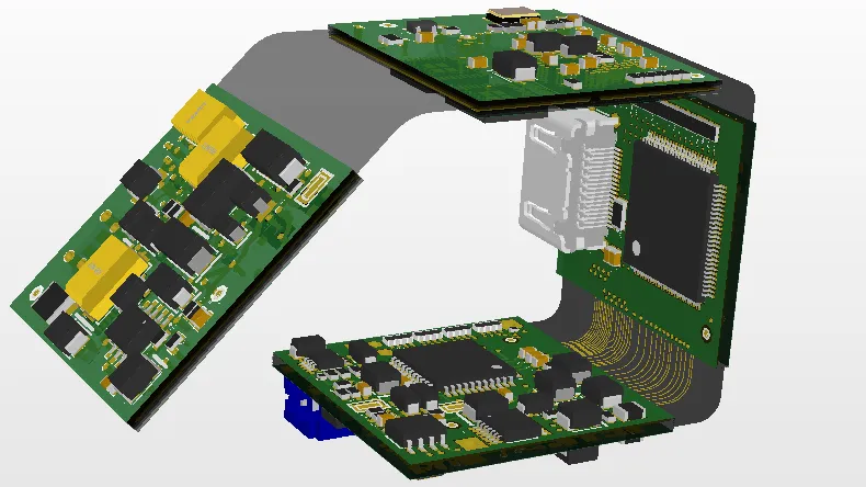
Why Choose Embedded Components for Your PCB Design?
Embedding components offers several advantages over traditional PCB assembly methods. Here's why you might consider this approach:
- Space Savings: By placing components inside the PCB, you free up surface space for other elements or reduce the overall board size. This is crucial for compact devices like smartwatches or medical implants.
- Improved Signal Integrity: Shorter connection paths between embedded components reduce parasitic inductance and capacitance, leading to better signal integrity. For high-speed designs, this can lower signal delay by up to 20% in some cases.
- Enhanced Reliability: Components embedded within the PCB are less exposed to physical stress, vibration, and moisture, improving the durability of the final product.
- Reduced Assembly Costs: Embedding can lower the number of surface-mount assembly steps, cutting down on labor and material costs during production.
However, embedding components requires careful planning and adherence to PCB design guidelines to avoid manufacturing challenges or performance issues. Let’s explore the key practices for success.
Key PCB Design Guidelines for Embedding Components
Designing a PCB with embedded components is a complex process that demands precision. Below are essential PCB design guidelines to ensure your project is both functional and manufacturable.
1. Select the Right Components for Embedding
Not all components are suitable for embedding. Focus on small, low-profile passive components like resistors and capacitors with standard sizes (e.g., 0201 or 0402). Some active components, like small ICs, can also be embedded, but they often require additional thermal management considerations. Always check the component's datasheet for embedding compatibility, including maximum operating temperature and mechanical stress limits.
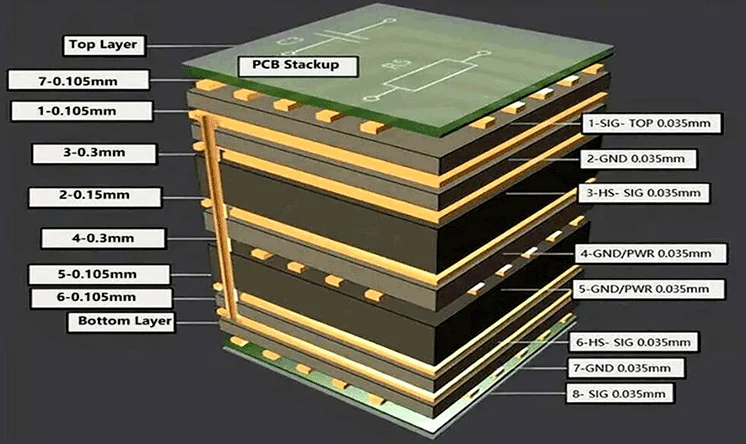
2. Understand Layer Stack-Up Requirements
Embedding components means integrating them into the internal layers of a multilayer PCB. Plan your layer stack-up carefully to accommodate the height and placement of embedded parts. For instance, a typical embedded capacitor might require a cavity or cutout in the dielectric layer, adding about 0.1 mm to 0.2 mm of thickness to that layer. Ensure your design software supports accurate 3D modeling of these layers to avoid alignment issues during fabrication.
3. Follow Embedded Component Design Rules
Adhering to embedded component design rules is critical for reliability. Some key rules include:
- Maintain a minimum clearance of 0.15 mm between embedded components and surrounding copper traces to prevent short circuits.
- Ensure via-in-pad designs for connecting embedded components to other layers, using microvias with diameters as small as 0.1 mm for high-density designs.
- Avoid placing embedded components near high-stress areas like board edges or mounting holes to reduce mechanical failure risks.
4. Optimize for Thermal Management
Embedded components can generate heat within the PCB, which is harder to dissipate than with surface-mounted parts. Use thermal vias or copper planes to conduct heat away from embedded components. For example, a thermal via array with a 0.3 mm diameter and 1.2 mm pitch can effectively manage heat in a 4-layer board with embedded ICs.
Design for Manufacturability (DFM) in Embedded PCB Layout
Design for manufacturability (DFM) ensures that your PCB layout with embedded components can be produced efficiently and without defects. Ignoring DFM principles can lead to increased costs, delays, or even board failures. Here are critical DFM considerations for embedding components.
1. Collaborate with Your Manufacturer Early
Embedding components often requires specialized manufacturing processes, such as laser drilling for cavities or precise lamination for multilayer alignment. Share your design files with your fabrication partner early to confirm their capabilities. For instance, ensure they can handle cavity depths of 0.2 mm to 0.5 mm for embedding standard passives.
2. Minimize Design Complexity
While embedding saves space, overly complex designs can complicate manufacturing. Limit the number of embedded components per layer to maintain alignment accuracy during lamination. A general rule is to embed no more than 10-15 components per square inch in a single layer to avoid registration errors.
3. Use Standard Materials and Processes
Opt for widely available PCB materials like FR-4 or high-Tg laminates that support embedding. Avoid exotic materials unless absolutely necessary, as they can increase costs by up to 30% and extend lead times. Similarly, stick to standard cavity sizes and shapes (e.g., rectangular cutouts) to simplify the manufacturing process.
PCB Layout with Embedded Components: Step-by-Step Process
Creating a successful PCB layout with embedded components requires a structured approach. Follow these steps to streamline your design process.
Step 1: Schematic Design and Component Selection
Start by creating a schematic that identifies which components will be embedded. Choose components with embedding-friendly packages and note their placement requirements in the schematic annotations. This helps during the layout phase to avoid placement conflicts.
Step 2: Define Layer Stack-Up and Cavities
In your design software, define the PCB layer stack-up, specifying where embedded components will reside. Create cavities or recesses in the appropriate layers to house these components. For example, a 0402 capacitor might need a cavity depth of 0.15 mm and a width of 0.6 mm.
Step 3: Placement and Routing
Place embedded components strategically to minimize signal path lengths and avoid interference with other layers. Use microvias for connections, ensuring a via aspect ratio of no more than 0.8:1 (e.g., a 0.1 mm diameter via in a 0.125 mm thick layer) to maintain reliability. Route traces with controlled impedance, targeting values like 50 ohms for high-speed signals.
Step 4: Validation and Simulation
Run design rule checks (DRC) and simulations to verify signal integrity and thermal performance. Check for issues like crosstalk or excessive heat buildup near embedded components. Simulation tools can predict impedance mismatches, helping you adjust trace widths (e.g., from 0.1 mm to 0.15 mm) if needed.
Altium Embedded Component Design: Tips and Tools
For engineers using popular design software, mastering Altium embedded component design can significantly enhance your workflow. This platform offers robust tools for integrating embedded components into your PCB layout. Here are some best practices:
1. Use 3D Modeling Features
The software’s 3D view allows you to visualize embedded components within the PCB layers. This helps ensure proper alignment and cavity sizing. For instance, you can set a component height of 0.2 mm and confirm it fits within the designated layer thickness.
2. Leverage Design Rule Checks (DRC)
Set custom rules in the software for embedded component clearances and via sizes. For example, configure a rule to flag any clearance less than 0.15 mm between embedded parts and nearby traces, preventing potential shorts during manufacturing.
3. Utilize Library Management
Create or import component libraries with predefined embedded footprints. This saves time and ensures consistency across designs. Tag components as "embedded" in the library to quickly filter them during placement.
Common Challenges and How to Overcome Them
Embedding components in PCBs comes with unique challenges. Here’s how to address some common issues:
- Alignment Errors: Misalignment during lamination can shift embedded components. Use fiducial markers on each layer to ensure precise registration, targeting an alignment tolerance of ±0.05 mm.
- Thermal Stress: Excessive heat during soldering or operation can damage embedded parts. Incorporate thermal vias and simulate heat dissipation to keep temperatures below 85°C for most passives.
- Cost Overruns: Embedding often increases fabrication costs due to specialized processes. Balance the number of embedded components with budget constraints, focusing on high-impact areas like signal-critical zones.
Conclusion: Mastering Embedded Component Design
Integrating components within PCBs is a powerful way to achieve compact, high-performance designs. By following the PCB design guidelines and embedded component design rules outlined in this post, you can create layouts that meet both functional and manufacturability goals. Emphasizing design for manufacturability (DFM) ensures your PCB layout with embedded components is ready for production, while tools supporting Altium embedded component design streamline the process with precision.
Start small by embedding a few passive components in your next project, and gradually scale up as you gain confidence. With careful planning and the right strategies, you can unlock the full potential of embedded design for your electronics. Trust in proven practices and collaboration with your manufacturing partner to bring your innovative designs to life.


