ALLPCB


Overview
The search for faster, lower-cost non-volatile memory alternatives has renewed interest in resistive RAM (ReRAM), especially for automotive and other embedded applications. Embedded flash has long frustrated designers seeking higher write speeds and lower energy use. As flash scaling advantages diminish near 28 nm, manufacturing complexity and cost increase because flash may require many more masks. Flash also demands higher front-end thermal budget and relatively high voltages. These factors create opportunities for alternative memory technologies such as ReRAM.
Market Context
Memory markets are difficult for new technologies to penetrate because incumbents benefit from fully depreciated fabs and proven long-term reliability. New memory types are more likely to find initial footholds in higher-end segments of the NOR flash market, where ASPs are higher and heterogeneous integration is more common, rather than immediately replacing mainstream NOR in all applications.
Automotive is a notable example, since cost and reliability are critical. The use of flash in vehicles has increased with the rise of wireless imaging and multiple firmware images per vehicle for redundancy and rollback protection. ReRAM proponents argue some new use cases need higher performance that flash scaling alone cannot provide.
Industry Viewpoints
Advocates say ReRAM can serve as embedded storage in IoT devices or as a discrete memory for MCUs. ReRAM is immune to magnetic attacks, which may suit special environments or security-sensitive applications. Ultimately, NVM choices will depend on trade-offs in performance, power, reliability, density, form factor, and cost; there is no single universal solution.
Market research shows differing trajectories: Business Market Insights projects NOR market growth at about 14% CAGR to reach $1.64 billion by 2028. Data Bridge Market Research forecasts ReRAM growing faster, at about 17.2% CAGR to reach $2.16 billion by 2030. Many companies remain bullish on multiple NVM technologies given heterogeneous integration and rising data demand.
Recent Developments and Adoption
ReRAM has matured in recent years after earlier setbacks. Companies and startups have resolved many materials challenges to produce consistent device behavior. Academic and industry labs have adopted ReRAM demonstrations for neuromorphic AI applications, as seen in collaborative research projects.
Different vendors have pursued different material systems. IBM has worked with hafnium oxide (HfO2), leveraging prior experience with hafnium-based gate dielectrics. Other entrants have used silicon oxide variants and engineered oxide layers to create switchable resistance states.
ReRAM is now being qualified in several manufacturing processes. For example, Weebit Nano’s ReRAM has been qualified for SkyWater Technology’s 130 nm CMOS process. TSMC and Infineon have also collaborated on ReRAM integration and adopted it for automotive microcontrollers. ReRAM has advantages for secure payment and identification cards thanks to radiation hardness and electromagnetic tolerance.
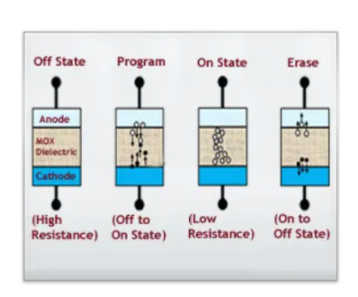
How ReRAM Works
ReRAM uses resistance changes rather than charge storage to represent data. The basic element is a variable resistor whose resistance can be changed by applying specific voltages and then reset or set again. Two main classes are OxRAM and CBRAM.
- OxRAM: A metal oxide layer between two electrodes forms conductive filaments composed of oxygen vacancies when a suitable polarity is applied. Reversing the polarity dissolves the filament, switching the cell between low-resistance and high-resistance states.
- CBRAM: Metal ions, typically copper or silver, migrate into a solid electrolyte to form a conductive bridge between electrodes. Dissolving the bridge returns the cell to a high-resistance state.
Advantages
Compared with embedded flash, ReRAM can require fewer masks for CMOS integration, scale to smaller nodes, and be byte-addressable, enabling direct writes rather than block-based updates. Because it is not charge-based, ReRAM avoids charge leakage issues. For some applications, ReRAM’s simpler stack and potential lower cost make it attractive.
Technical Challenges
ReRAM faces several technical limitations.
- Variability and noise: ReRAM devices exhibit intrinsic variability due to the stochastic nature of filament formation and dissolution. Small numbers of oxygen vacancies or metal atoms can cause large resistance swings, producing significant cycle-to-cycle and device-to-device variability. This results in higher noise compared with some other memories.
- Thermal sensitivity: Self-heating and temperature variations can impact the resistance ratio between states and thereby affect accuracy and reliability, particularly in dense or high-power designs. Careful thermal management and multi-physics modeling are required to predict chip-level thermal evolution and its effects.
- Modeling gaps: There is a lack of comprehensive quantitative multi-physics models (electrical, thermal, chemical) that capture filament dynamics and variability. Empirical models exist, but limited fundamental physics makes process control and optimization harder.
- Write speed and endurance: Typical ReRAM write times are substantially slower than SRAM; reported write times can be in the microsecond to tens of microseconds range, and targeted endurance levels are often around 1e5 cycles, which is insufficient for last-level caches that require up to 1e12 cycles. Some vendors report faster ReRAM variants with nanosecond-scale writes, but MRAM demonstrations still show significantly faster switching in certain settings.
Positioning vs MRAM, Flash and Others
ReRAM is viewed as a leading candidate to replace high-end embedded flash but is less competitive against NAND for cost-per-bit. MRAM remains an important alternative: MRAM generally offers higher performance but at a higher process cost. ReRAM proponents point to simpler fabrication and wider read windows compared with MRAM, which can ease yield control. MRAM’s speed and endurance profile make it a stronger candidate for cache applications, while ReRAM may find roles in embedded storage and certain secure or radiation-tolerant domains.
Outlook
Multiple NVM options are likely to coexist in the foreseeable future, each tailored to specific application trade-offs in speed, endurance, power, cost, and integration complexity. Rather than a single universal NVM, the trend is toward application-specific selection and heterogeneous integration.
In summary, ReRAM shows potential to replace NOR flash in selected embedded and automotive use cases where its attributes align with system requirements, but technical challenges in variability, thermal behavior, write speed, and modeling mean it will complement rather than universally displace existing NVM technologies for now.