 ALLPCB


In the world of high-speed PCB design, signal integrity is everything. One of the biggest challenges designers face is managing via stubs—unused portions of through-hole vias that can disrupt signals and degrade performance. So, how do you solve this problem? PCB backdrilling, also known as controlled depth drilling, is the answer. This technique removes via stubs to improve signal integrity, making it a must for high-speed applications. In this ultimate guide, we’ll dive deep into backdrilling design, covering everything from the basics of via stub removal to advanced tips for optimizing your high-speed PCB layouts.
Whether you're searching for a PCB backdrilling tutorial or looking to understand signal integrity improvement, this blog will walk you through the process, benefits, and best practices for controlled depth drilling. Let’s get started!
What Are Via Stubs and Why Do They Matter in High-Speed PCB Design?
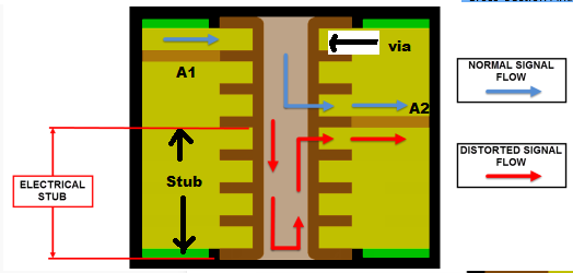
In printed circuit boards (PCBs), vias are small holes that connect different layers, allowing signals to travel through the board. However, when a via extends beyond the layers it needs to connect, the unused portion is called a via stub. These stubs act like tiny antennas, causing signal reflections, noise, and impedance mismatches. For low-speed designs, this might not be a big issue. But in high-speed PCB design, where signals often exceed 3 Gbps, via stubs can severely impact performance.
For example, a via stub as short as 0.5 mm can cause significant signal distortion at frequencies above 5 GHz. This distortion leads to data errors, increased jitter, and reduced system reliability. Removing these stubs through backdrilling is critical for maintaining clean signal transmission and achieving signal integrity improvement.
What Is PCB Backdrilling and How Does It Work?
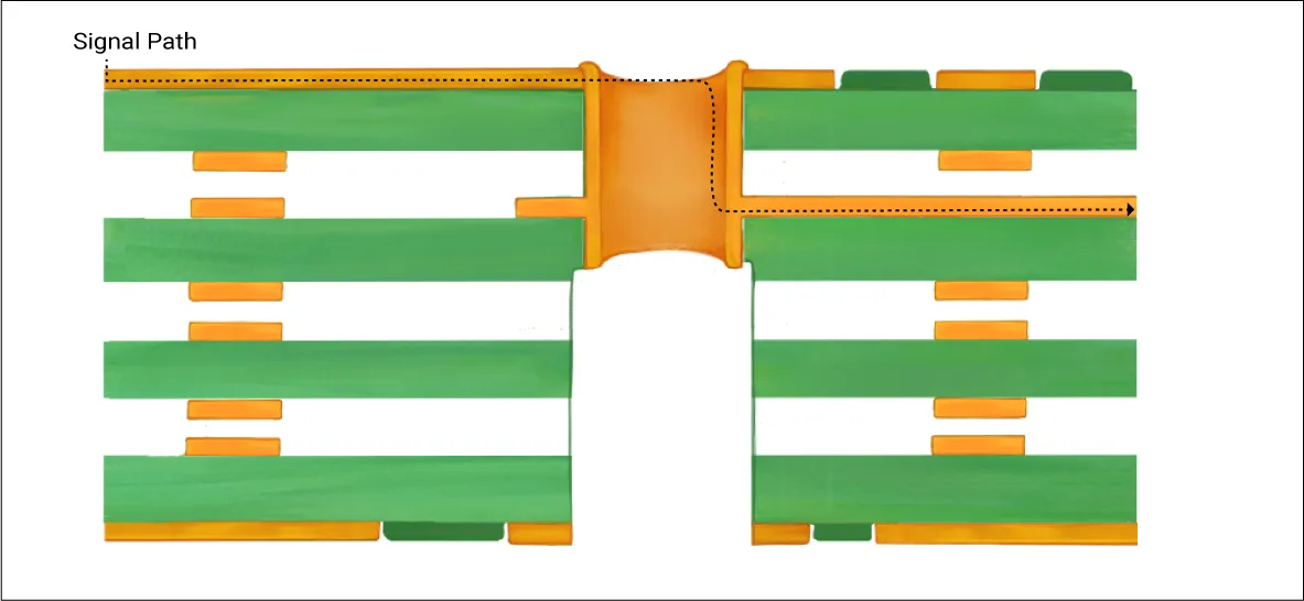
PCB backdrilling, or controlled depth drilling, is a manufacturing technique used to remove the unused portion of a via stub after the initial drilling and plating process. It involves drilling a slightly larger hole from the opposite side of the board to eliminate the stub without damaging the functional part of the via.
Here’s a simplified step-by-step process of how backdrilling works:
- Initial Via Creation: A through-hole via is drilled and plated to connect specific layers of the PCB.
- Stub Identification: The unused portion of the via (the stub) below or above the connected layers is identified.
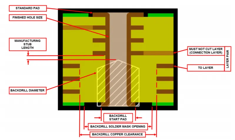
- Controlled Depth Drilling: A larger drill bit removes the stub, stopping at a precise depth to avoid damaging the active via barrel. Modern equipment achieves tolerances as tight as ±0.05 mm.
- Final Inspection: The board is checked to ensure the stub is removed and the via remains functional.
Backdrilling is especially important for high-speed PCB designs because it minimizes signal loss and reduces electromagnetic interference (EMI). By eliminating via stubs, you can achieve cleaner signal paths and better overall performance.
Why Is Backdrilling Crucial for Signal Integrity Improvement?
Signal integrity refers to the quality of an electrical signal as it travels through a PCB. In high-speed designs, maintaining signal integrity is vital to prevent data loss and ensure reliable communication. Via stubs are a major obstacle because they create unwanted reflections and resonate at specific frequencies, distorting the signal.
For instance, a via stub can cause a resonance peak at around 10 GHz, leading to a signal loss of up to 3 dB or more. Backdrilling eliminates this issue by removing the stub, resulting in smoother impedance transitions and reduced noise. This is especially critical for applications like telecommunications, data centers, and high-speed digital systems where even small signal disruptions can lead to significant problems.
The benefits of backdrilling for signal integrity improvement include:
- Reduced Signal Reflections: Eliminating stubs minimizes bounce-back effects that distort signals.
- Lower Crosstalk: Cleaner signal paths reduce interference between adjacent traces.
- Improved Impedance Matching: Removing stubs helps maintain consistent impedance, often targeting values like 50 ohms for high-speed signals.
- Enhanced Data Rates: Backdrilling supports higher data rates, making it ideal for designs exceeding 10 Gbps.
When Should You Use Backdrilling in High-Speed PCB Design?
Not every PCB design requires backdrilling. It’s typically reserved for high-speed applications where signal integrity is a priority. Here are some scenarios where backdrilling is essential:
- High-Speed Digital Signals: Designs with data rates above 3 Gbps, such as DDR4 memory or PCIe interfaces, often need backdrilling to maintain performance.
- Thick Multilayer Boards: Boards with 12 or more layers are more likely to have long via stubs that impact signal quality.
- RF and Microwave Applications: In designs operating at frequencies above 1 GHz, via stubs can cause significant signal loss, making backdrilling necessary.
If your design operates at lower speeds or has minimal layer transitions, you might not need backdrilling. However, for cutting-edge technology where every bit of performance matters, this technique is a game-changer.
Key Design Guidelines for Effective PCB Backdrilling
To achieve the best results with backdrilling, you need to follow specific design rules. These guidelines ensure manufacturability and optimize signal integrity improvement. Here are some essential tips for your high-speed PCB design:
1. Identify Critical Vias
Not all vias need backdrilling. Focus on those carrying high-speed signals or connecting to critical components. Use simulation tools to analyze which vias have stubs that could impact performance at your operating frequencies.
2. Specify Backdrill Depth and Tolerance
Precision is key in controlled depth drilling. Define the exact depth for backdrilling in your design files, ensuring the drill stops just before the functional via barrel. Typical tolerances are ±0.05 mm to avoid damaging the via or leaving residual stubs.
3. Use Larger Backdrill Diameters
The backdrill bit should be slightly larger than the original via diameter (usually 0.15-0.25 mm larger) to ensure complete stub removal without affecting the via’s plated barrel.
4. Minimize Stub Length in Design
Even with backdrilling, aim to keep via stubs as short as possible during the initial layout. Route high-speed signals to inner layers closer to the surface to reduce stub length before backdrilling.
5. Collaborate with Your Manufacturer
Backdrilling requires advanced equipment and expertise. Work closely with your PCB fabrication team to confirm their capabilities, such as depth control accuracy and supported board thicknesses. Provide clear documentation, including backdrill layers and depths, in your design files.
Benefits of Backdrilling for High-Speed PCB Design
Implementing backdrilling in your PCB design offers several advantages beyond just via stub removal. Here’s why it’s worth considering for your next project:
- Enhanced Signal Quality: Cleaner signals mean fewer errors and higher reliability, especially at data rates above 5 Gbps.
- Cost-Effective Solution: While backdrilling adds a manufacturing step, it’s often more affordable than redesigning a board or using complex alternatives like blind vias.
- Supports Complex Designs: Backdrilling makes it easier to manage signal integrity in multilayer boards with 16 or more layers.
- Reduced EMI: Removing stubs lowers electromagnetic interference, which is crucial for meeting regulatory standards in sensitive applications.
Challenges and Limitations of PCB Backdrilling
While backdrilling is a powerful technique, it’s not without challenges. Understanding these limitations can help you plan your design more effectively:
- Manufacturing Precision: Achieving tight depth tolerances requires advanced equipment, and not all manufacturers can perform backdrilling accurately.
- Increased Cost: Backdrilling adds an extra step to the fabrication process, which can raise costs, especially for small production runs.
- Design Complexity: Identifying which vias need backdrilling and specifying depths can complicate the design process, requiring additional simulation and planning.
- Not Suitable for All Boards: Thin boards or designs with minimal stubs may not benefit from backdrilling, and the process could even risk damaging the via if not done carefully.
Alternatives to Backdrilling for Via Stub Removal
If backdrilling isn’t feasible for your project due to cost or manufacturing constraints, there are alternative methods to manage via stubs in high-speed PCB design:
- Blind and Buried Vias: These vias only connect specific layers without extending through the entire board, eliminating stubs altogether. However, they are more expensive to manufacture.
- Via-in-Pad Design: Placing vias directly under component pads can reduce stub length, though this requires careful thermal management.
- Signal Layer Planning: Route high-speed signals on layers closer to the board surface to minimize stub length naturally.
While these alternatives can be effective, backdrilling often remains the most practical and cost-efficient solution for many high-speed designs.
Real-World Applications of Backdrilling in High-Speed PCB Design
Backdrilling is widely used across industries where high-speed performance is non-negotiable. Here are a few examples of its real-world applications:
- Telecommunications: High-speed routers and switches rely on backdrilling to handle data rates of 25 Gbps and beyond with minimal signal loss.
- Data Centers: Server boards processing massive data volumes use backdrilling to ensure reliable communication between components.
- Aerospace and Defense: Systems requiring low EMI and high reliability, such as radar and communication equipment, benefit from backdrilling to meet strict performance standards.
How to Get Started with Backdrilling: A PCB Backdrilling Tutorial
Ready to incorporate backdrilling into your next high-speed PCB design? Follow these actionable steps to ensure success:
- Analyze Your Design: Use simulation software to identify vias with stubs that could affect signal integrity at your target frequencies.
- Define Backdrill Parameters: Specify the depth, diameter, and location of backdrills in your design files. Include a separate layer or documentation for clarity.
- Consult Your Fabricator: Confirm that your manufacturing partner supports controlled depth drilling and discuss their specific requirements or limitations.
- Test and Validate: After fabrication, perform signal integrity tests to verify that stub removal has improved performance as expected.
By following these steps, you can seamlessly integrate backdrilling into your workflow and achieve significant signal integrity improvement.
Conclusion: Mastering Backdrilling for High-Speed PCB Success
Backdrilling is a vital technique for anyone involved in high-speed PCB design. By eliminating via stubs through controlled depth drilling, you can dramatically enhance signal integrity, reduce noise, and support faster data rates. Whether you’re working on telecommunications equipment, data center servers, or other cutting-edge technology, mastering backdrilling design can give your projects a competitive edge.
This guide has covered everything from the basics of via stub removal to practical design tips and real-world applications. By applying these insights, you’re well on your way to creating high-performance PCBs that meet the demands of modern electronics. Remember to collaborate closely with your manufacturing team and use simulation tools to fine-tune your designs for optimal results.
With backdrilling, you’re not just improving signal paths—you’re building the foundation for reliable, high-speed innovation.


