 ALLPCB


If you're dealing with PCB gold finger plating defects like peeling, corrosion, or discoloration, you're not alone. These issues can disrupt the reliability of your circuit boards, leading to poor connections and costly failures. In this guide, we'll walk you through the most common problems—gold finger peeling, gold finger corrosion, gold finger discoloration, poor gold finger adhesion, and gold finger plating thickness issues—and provide practical solutions to troubleshoot and prevent them. Whether you're a PCB designer or manufacturer, this detailed resource will help you ensure high-quality edge connectors for your projects.
What Are PCB Gold Fingers and Why Do They Matter?
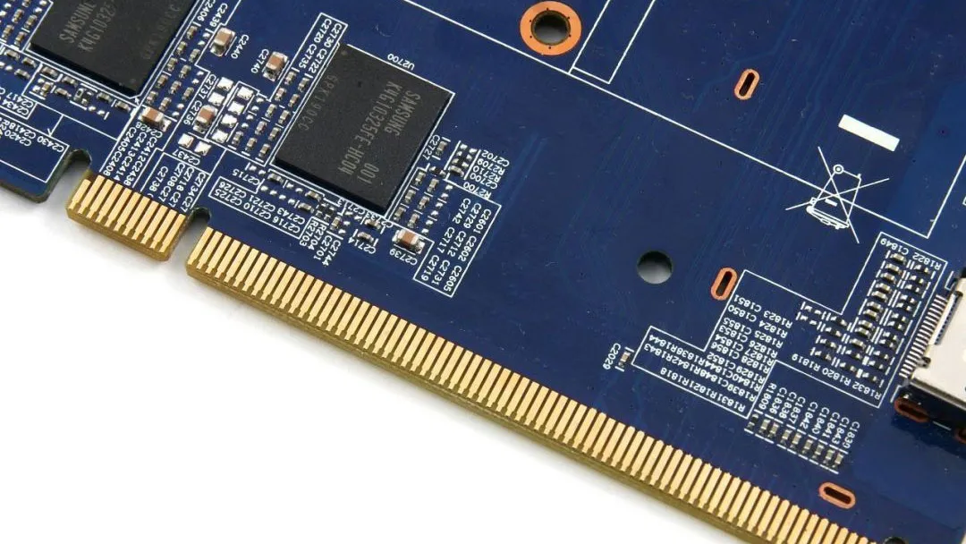
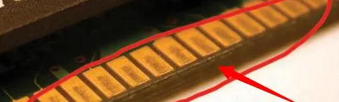
Gold fingers, also known as edge connectors, are the gold-plated pads located along the edges of a printed circuit board (PCB). They serve as the interface for connecting the PCB to other devices, such as motherboards or expansion slots. Gold is used for its excellent conductivity (with a resistivity of about 2.44 × 10^-8 Ω·m) and resistance to corrosion, ensuring reliable signal transmission even in high-frequency applications (up to several GHz in some cases).
However, defects in gold finger plating can compromise these benefits, leading to signal loss, intermittent connections, or complete failure. Identifying and resolving issues like peeling or uneven thickness is critical to maintaining the performance of your PCBs, especially in industries like telecommunications, aerospace, and consumer electronics where reliability is non-negotiable.
Common Issues in PCB Gold Finger Plating
Gold finger plating defects can stem from various stages of the manufacturing process, environmental factors, or design oversights. Below, we dive into the most frequent problems and their root causes.
1. Gold Finger Peeling
What It Is: Gold finger peeling occurs when the gold layer separates from the underlying nickel or copper substrate, often visible as flaking or lifting at the edges of the connector.
Common Causes:
- Poor Surface Preparation: If the PCB surface isn’t properly cleaned or roughened before plating, adhesion between layers suffers.
- Inadequate Nickel Underlayer: A nickel layer (typically 3-5 micrometers thick) acts as a barrier and adhesion promoter. If it’s too thin or uneven, the gold layer may not bond well.
- Contamination: Residues like oils or dust on the board during plating can weaken the bond.
Troubleshooting Tips:
- Ensure thorough cleaning and micro-etching of the PCB surface before plating to remove oxides and contaminants.
- Verify the nickel layer thickness using cross-sectional analysis or X-ray fluorescence (XRF) testing. Aim for a consistent 3-5 micrometers.
- Use a controlled environment during plating to minimize dust and humidity, which can introduce contaminants.
2. Gold Finger Corrosion
What It Is: Gold finger corrosion appears as tarnish or pitting on the gold surface, often due to exposure to harsh environments or poor plating quality.
Common Causes:
- Porous Gold Layer: If the gold plating is too thin (below 0.5 micrometers for soft gold), it may not fully protect the underlying nickel, allowing corrosion to occur.
- Environmental Exposure: High humidity, salt spray, or sulfur-containing atmospheres can penetrate weak spots in the plating.
- Improper Storage: Storing PCBs without protective packaging can expose gold fingers to corrosive elements.
Troubleshooting Tips:
- Measure gold thickness using XRF or other non-destructive testing methods. For hard gold, aim for 0.8-1.5 micrometers; for soft gold, 0.5-0.8 micrometers is often sufficient.
- Apply a conformal coating or use anti-tarnish treatments on gold fingers if the PCB will be exposed to harsh conditions.
- Store finished PCBs in moisture-proof bags with desiccants to prevent environmental damage.
3. Gold Finger Discoloration
What It Is: Gold finger discoloration manifests as uneven or abnormal coloring of the gold layer, such as reddish or brownish hues instead of the typical bright yellow-gold.
Common Causes:
- Impure Gold Bath: Contaminants in the plating solution, like copper or organic residues, can alter the gold’s appearance.
- Nickel Diffusion: If the gold layer is too thin, nickel can diffuse to the surface over time, causing a dull or discolored look.
- Oxidation: Exposure to air or heat during manufacturing can oxidize underlying layers, affecting the gold’s color.
Troubleshooting Tips:
- Regularly test and filter the plating bath to remove impurities. Maintain strict control over bath chemistry, including pH (typically 4.0-4.5 for gold plating) and temperature (around 50-60°C).
- Ensure adequate gold thickness to prevent nickel diffusion. A minimum of 0.5 micrometers is recommended for most applications.
- Minimize exposure to high temperatures during soldering or reflow processes near the gold fingers.
4. Poor Gold Finger Adhesion
What It Is: Poor gold finger adhesion refers to weak bonding between the gold layer and the substrate, leading to delamination or peeling under mechanical stress or thermal cycling.
Common Causes:
- Inadequate Surface Roughness: A smooth surface reduces the mechanical interlocking needed for strong adhesion.
- Improper Plating Parameters: Incorrect current density (typically 1-3 A/dm2 for gold plating) or bath temperature can result in weak deposits.
- Substrate Issues: Defects in the copper or nickel underlayers can prevent proper adhesion of the gold.
Troubleshooting Tips:
- Use micro-etching to create a slightly rough surface (Ra value of 0.5-1.0 micrometers) before plating for better mechanical bonding.
- Monitor and adjust plating parameters, ensuring current density and bath conditions are within recommended ranges.
- Inspect the nickel and copper layers for defects using microscopic analysis before applying the gold layer.
5. Gold Finger Plating Thickness Issues
What It Is: Gold finger plating thickness issues occur when the gold layer is either too thin, leading to wear and corrosion, or too thick, increasing costs and risking cracking.
Common Causes:
- Inconsistent Plating Process: Variations in current distribution or bath agitation can lead to uneven thickness across the gold fingers.
- Insufficient Monitoring: Lack of real-time measurement during plating can result in over- or under-plating.
- Design Oversights: Poor panel layout or spacing can cause uneven current flow, affecting thickness uniformity.
Troubleshooting Tips:
- Use plating equipment with uniform current distribution and proper agitation to ensure consistent thickness (target range: 0.5-1.5 micrometers depending on application).
- Implement in-process monitoring with tools like XRF to measure thickness during plating and make adjustments as needed.
- Optimize PCB panel design to avoid shadowing effects or uneven current density at the edges where gold fingers are located.
Preventive Measures for Reliable Gold Finger Plating
While troubleshooting is essential, preventing PCB gold finger plating defects in the first place saves time and resources. Here are some best practices to ensure high-quality plating:
- Strict Process Control: Maintain consistent plating bath conditions, including temperature, pH, and current density, to avoid variations in quality.
- Quality Materials: Use high-purity gold and nickel solutions to prevent contamination and ensure a durable finish.
- Regular Testing: Perform adhesion tests (like tape testing per IPC-TM-650 standards) and thickness measurements after plating to catch issues early.
- Design Optimization: Incorporate beveling (typically at a 30-45-degree angle) on gold fingers to reduce wear during repeated insertions and ensure smooth connections.
- Environmental Protection: Package finished PCBs in anti-static, moisture-proof materials to protect gold fingers during storage and shipping.
How to Inspect and Test Gold Finger Plating Quality
Regular inspection and testing are key to identifying defects before they cause failures. Here are some practical methods to evaluate gold finger quality:
- Visual Inspection: Use a magnifying glass or microscope (10x-20x magnification) to check for discoloration, peeling, or pitting on the gold surface.
- Thickness Measurement: Employ XRF or coulometric testing to confirm that gold thickness meets specifications (e.g., 0.5-1.5 micrometers).
- Adhesion Testing: Perform a tape test or thermal cycling test to ensure the gold layer withstands mechanical and environmental stress.
- Corrosion Resistance: Conduct salt spray testing (per MIL-STD-883 standards) to simulate harsh environments and verify the gold layer’s protective capability.
Conclusion: Achieving Flawless Gold Finger Plating
Dealing with PCB gold finger plating defects like gold finger peeling, gold finger corrosion, gold finger discoloration, poor gold finger adhesion, and gold finger plating thickness issues can be challenging, but with the right approach, these problems are solvable. By understanding the root causes, implementing strict process controls, and conducting thorough inspections, you can ensure reliable and durable gold fingers for your PCBs. At ALLPCB, we’re committed to supporting your projects with high-quality manufacturing solutions tailored to prevent such issues and deliver exceptional results.
With this practical guide, you now have the tools to troubleshoot and prevent common gold finger plating problems. Apply these tips to your next project, and enjoy the benefits of consistent, high-performance edge connectors.


